Tuesday, July 3, 2012

Photobit PB-0100-5 teardown

Earlier today I was cleaning out a drawer in my lab and found a broken USB webcam. Before throwing it out I decided to desolder the sensor chip and have a look.

For those of you who aren't familiar with it, my friend John and I are the driving forces between the Silicon Pr0n project - a wiki dedicated to amassing knowledge about all things related to semiconductor RE. I haven't been doing as much work on it recently due to academic obligations but figured it was about time to post some more die photos!

Wiki page: http://siliconpr0n.org/archive/doku.php?id=azonenberg:photobit:pb0100

Map: http://siliconpr0n.org/map/photobit/pb-0100-5/neo5x/ 

Package shots after removing from the board:

Top view of sensor
Bottom view
The package is a ceramic LGA using gold ball bonding. I have so far made no attempt to remove the die from the package or delayer; all images were taken through the window on the front of the package.

Without even resorting to the microscope some structure is obvious:
  • The red and green area at the upper left of the die is the pixel array.
  • The remainder of the die is covered with a transparent blue material (which upon closer inspection looks exactly like the blue color filter in the pixels) to prevent photocurrents from messing up the control logic
  • The area below the sensor has a lot of fine detail and is irregular. It's probably an array of standard logic cells controlling the sensor readout.
  • The area to the right of the sensor looks very regular and is probably addressing logic, buffers, and the ADCs.
  • Several of the pins along the top and left edge have three bond wires instead of one. They're probably power/ground.
  • Not all bond pads are broken out to pins.
I made an imaging pass over the entire die with a 5x objective. Since I haven't had time to do a CNC mod on my microscope stage like John has, I have to move the stage and snap photos by hand. This makes high-magnification full-die imaging very time consuming so if I need that I'll usually send the chip to him for processing.

Without further ado here's the full-die image. Note that this is rotated 90 degrees clockwise from the package overview image so that the vendor logo is right side up.

Full-die image
Closer inspection reveals that the standard cell area at left has large spaces between rows of logic for interconnect, suggesting that this is a 2-metal design. As typical for 1999-era technology the metal layers are not planarized. Sub-pixels look to be about 5 μm across.

Random portion of the subpixel array
The bottom right of the die has the Photobit logo and copyright notice:

Vendor logo and copyright. Note probe scrub mark from wafer test on the upper right pad.
Right above the logo there were a bunch of ID markings from the individual masks. It's immediately obvious that several masks are not visible as there are gaps in the array. These are probably the implants.

Several metal layers are visible, along with at least one polysilicon and several whose purpose is not immediately obvious.

Mask ID markings
The most interesting feature observed was at the bottom left of the die - a little doodle of a panda bear snuck in by the layout engineer.

Mask art!

Sunday, July 1, 2012

BGA process notes

I've gotten a lot of requests recently to share some details on my BGA assembly process, so without further ado here it is!

The board in this example is a test vehicle with an 11x11 0.8mm XBGA footprint on it, being mounted with a PIC32MX engineering sample chip. This is the same board I used in my 0201 process test.

I deliberately put several unfilled vias in the pads to demonstrate why this is a bad idea. Keep reading for details!

0.8mm XBGA test vehicle. Black marker lines highlight the row of balls that will be used for the cross section.
Since I don't have in-house stencil capabilities and haven't gotten around to ordering professionally made ones, I do all of my BGAs with flux only. My preferred flux for this purpose is ChipQuik SMD291NL no-clean rosin tack flux.

BGA pads covered in flux
The next step is to position the BGA on top of the footprint. Well-made footprints (such as the 256-FTBGA that I use on most of my FPGA boards) have the silkscreen outline slightly larger than the chip. Unfortunately this one is the same size as the chip so it was very difficult to align properly. I tried my best but it was still a little off.

BGA on footprint
I then ran the board through the standard reflow profile in my toaster oven. It's a cheap Proctor-Silex oven purchased at WalMart for something like $25. There is no thermocouple or feedback circuit in it (I have a 120VAC rated relay and a thermocouple but have not hooked it up yet.)
  • Set to 90C for 3 minutes to preheat
  • Set to 150C for 1 minute for thermal soak.
  • Set to 210C for 1 minute for reflow. This results in a Tal of about 15 seconds.
  • Turn off oven, open door, and cool to ambient with room air
Note that these numbers are not intended to describe the actual temperatures reached by the board or the oven - they're just the numbers on the dial of my specific oven. I know for a fact that the peak temperature reached at the 210C setting is in excess of 220C because that's the melting point of SAC305 solder.

I've also heard of people using oven thermometers to calibrate their reflow ovens. One word of caution for those doing this - if your sensor has a significantly higher thermal mass than your board (such as a big metal oven thermometer) its temperature will lag behind that of the less-massive PCB by a significant amount. I know of at least one hobbyist who reached the thermal decomposition point of FR4 Tg170 (somewhere around 300C) when his thermometer showed only 260!

The best way to tell when reflow is complete on an un-calibrated oven like mine is to watch the solder melt. My paste changes from a glossy gray (full of volatile flux compounds) to matte gray (once most of the flux has boiled off) to shiny silver (after the solder melts); BGA balls turn from a dull metallic color to shiny silver at melting; the chip also sinks slightly as the balls flatten from the weight of the IC. This YouTube video (not from my lab) shows what a properly reflowing BGA looks like.

The test vehicle in the oven. Note scrap-grade 4-inch silicon wafer being used as "cookie sheet".
Since this was a test board with no actual circuitry on it, the next step was to prepare to cross-section it and look at how well the joints turned out.

Although the flux I used is no-clean (and I normally leave it in place on most of my boards) cross sections look nicer if there isn't *too* much flux in the way. Since I don't have an ultrasonic cleaner yet (I do plan to buy one in the near future) I just let it soak in a beaker of 70% isopropyl alcohol for a few minutes, shook around a bit, and wiped it dry.

PCB sitting in beaker of IPA in my fume hood. Although IPA isn't particularly dangerous as solvents go, I have a general policy of keeping all open solvent containers in the hood whenever possible.
Once the board was dry I cut it in half between the black lines with a Dremel and a cut-off wheel. My ShopVac-based dust control system works reasonably well, but I want to get a HEPA vac for this in the future.

After the rough cut I polished with 1200 grit sandpaper and wiped away the dust with a wet cloth. Upon looking under the microscope I saw that the failure I was hoping to demonstrate had indeed occurred - one of the balls had been sucked down into an uncapped via by capillary action, resulting in a complete lack of electrical contact. The ball at far right had been partially sucked into the via but the solder mask dam was big enough to keep it from going in all the way.

Cross section of PCB and BGA. Note solder-filled via in center and missing ball. The far-right via annular ring seems to have snagged on something during the cutting process and been ripped up off the board.

Looking to one side of the board it was clear that the balls without vias under them had reflowed properly and were reasonably well aligned.

The black material between the balls is not underfill, it's a paste-like material made of residual flux, FR4/molding compound dust, and little slivers of copper that were ground off by the sanding process. It looks like my defluxing process didn't work as well as I had hoped; I'm going to need ultrasound to do the job properly.

One very interesting and unexpected result was visible in this cross section - the next row of vias were visible through the FR4 laminate.

Three well-reflowed balls. Note vias in next row visible through laminate.
Before closing up the lab for the night I decided to take one last picture to show what an ENIG-finished via looks like. Since this was a higher magnification image I followed the sandpaper polish with 3μm diamond paste to get a better finish.

The layers visible in this image from bottom to top are FR4 (grayish), 1oz/35μm copper foil(copper) and what looks like about 10μm of nickel (yellow-gray).  The gold plating is too thin to see at this magnification.

Cross section of ENIG-finished via.

Friday, June 29, 2012

ISim bugs and introducing the RED TIN internal logic analyzer

Earlier this month I was working on a Spartan-6 based design using the on-chip DDR SDRAM controller (MCB) and ran into some problems.

For those of you not familiar with the MCB, it's a pipelined DDR/DDR2/DDR3 controller that exposes several (up to 2 full-duplex and 4 half-duplex, or 4 full-duplex) distinct ports to your RTL. Each port can be independently clocked and the order of operations between ports may be unpredictable due to this (a round-robin arbitration scheme is used under the hood after synchronization) but operations on a single port execute in FIFO order. My design only uses port 0 at the moment, 1/2/3 will probably be used for DMA at some point in the future.

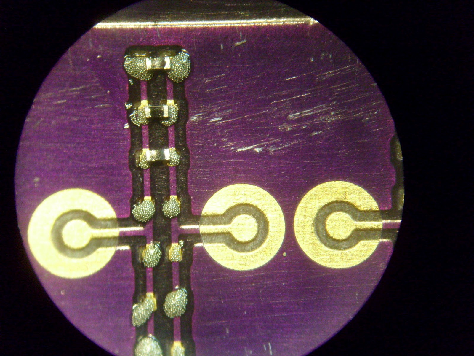
Each port consists of three FIFOs, which are capable of independent clocking but in practice typically share the same clock:
  • Command FIFO, which specifies the address, opcode (read, write, read with auto precharge, write with auto precharge), and burst length (number of words to write)
  • Write data FIFO, which stores data to be written plus a byte write-enable mask
  • Read data FIFO, which stores data read from RAM
To issue a write, push one or more data words and masks onto the write data FIFO and then push a write command onto the command FIFO. To read, push a read command and then read from the read data FIFO as it becomes available.

The read and write FIFOs are each 128 words deep, enough to accommodate most needs. Unfortunately, the command FIFO is much shallower - 4 commands. 

In deeply pipelined designs that do a lot of random-access operations such as my softcore CPU this isn't nearly enough! It's only exacerbated by the poor performance of the quick-and-dirty direct-mapped write-through L1 cache I'm using (I plan to replace it with a 2-way set-associative write-back cache at some point).

The obvious fix was to put a bigger FIFO in front of the MCB. This didn't work for some reason and I found myself reading garbage from memory. It wasn't clear where the bug was from reading the code, so I tried to simulate my design in ISim and take a closer look.

Being a hobbyist operating on a grad student's stipend doesn't leave me a lot of cash to spend on software so I try to stick with open source, or at least freeware, tools to the extent possible. The >$3K-per-seat ISE Design Suite Logic Edition is obviously not affordable so I use the freeware ISE WebPack for all of my FPGA designs.

WebPack includes the "Lite Edition" of ISim instead of the full version. According to the ISim FAQ page:
There is only one limitation. When the user design + testbench exceeds 50,000 lines of HDL code, the simulator will start to derate the performance of the simulator for that invocation... The line count includes both testbench and source code lines. The Xilinx libraries are not included in the line count.

I figured I was fine... my line-count script showed 10,129 lines of Verilog in my design directory (not all of which was being used in the simulation) plus another ~15k in the generated MCB code - well below 50k. As soon as I fired up the simulator, though, it slowed to a crawl and displayed a nag screen in the console:
This is a limited version of the ISE Simulator. The current design has exceeded the design size limit for this version and the performance of the simulation will be derated. Please contact your nearest sales office at www.xilinx.com/company/contact.htm or visit the Xilinx on-line store at www.xilinx.com/onlinestore/design_resources.htm if interested in purchasing the full, unlimited version of this simulator.
A binary search of my RTL (commenting out half of the file at a time) revealed that the MCB primitive was causing the line count to be hit. Despite the FAQ claiming that the Xilinx libraries are not included in the count, the MCB's behavioral model clearly is included.

Since the derated simulation was unusably slow (the millisecond or two required for calibration to complete would have taken several days of wall-clock time, before even starting to simulate my test suite) this was clearly not a viable option.

I started to look around for alternatives. The DDR chip was being clocked at 80 MHz DDR'd to 160 MT/s, too fast for my 100 MHz oscilloscope/LA to be of any help. Since the RAM was dynamic I couldn't slow it down. I only had 20 GPIO channels on the board, not nearly enough to bring out all of the signals of interest for probing (not that this was really a problem as the LA only had 16 channels).

The best option at this point looked to be Xilinx's ChipScope internal logic analyzer, which supports programmable triggers and can store a large number (their documentation isn't clear on exactly how many) of channels of data to on-chip memory, then stream to a PC over JTAG or Ethernet (or possibly other IO standards too). Unfortunately ChipScope is not included in a license. My options were to spend $695 on a node-locked license, $850 on a floating license, or $3000+ on a full Logic Edition ISE license.

Not having that kind of cash, I realized I was out of easy options - I was going to have to write my own tool. I sat down and started coding on an internal logic analyzer of my own, dubbed RED TIN (two words picked randomly from a dictionary - I'm terrible at coming up with names!).

A week and 2,063 lines of code later I had an alpha version ready for testing at http://code.google.com/p/red-tin-logic-analyzer/. It consists of four parts:
  • RedTinLogicAnalyzer, a Verilog core which handles the core capture/buffering code (currently hard-coded to 128 channels and 512 samples, will be parameterizable later on).
  • RedTinUARTWrapper, a wrapper around RedTinLogicAnalyzer that implements the board-to-PC protocol (the intention is to eventually support JTAG and other interfaces as well).
  • The redtin application, a C++/gtkmm GUI application which functions as the control panel of the logic analyzer
  • A third-party waveform viewer that can read standard vcd-format files. gtkwave is hard-coded in the alpha build but I'll provide an interface for using other viewers later on.
The capture code is portable Verilog and should work on any FPGA, though I've only tested on Spartan-6. The PC-side application is cross-platform except for the UART code, which is Linux-specific (I haven't yet had time to write a portable wrapper around that).

Using the core is pretty simple - just insert it into the design, feed up to 128 inputs into the "din" input, supply a clock, and connect the UART pins up to top-level pins on the FPGA. Note the 50 bits of zeros at the end to pad the total width up to 128 bits.


Without further ado, here's a screenshot of it in action!


It's a little hard to see in the small view (I have a quad-monitor setup on my desk, this is the left half) but the left side shows the control panel application (with iMPACT in the background) and the right side is data captured from one of my boards.

After a bit of poking around I found my bug!

While I was pushing write commands onto the extended FIFO, I had somehow forgotten to do so with reads. This resulted in a race condition where reads could either be stepped on by writes or, even worse, occur before the write had committed!

The above screenshot shows a write (p0_cmd_instr = 3'b000) executing after a read (p0_cmd_instr = 3'b001) even though the write was issued first (compare rising edge of wr to rising edge of read_active). As a result the read data was complete garbage (32'hDFBDBFEF instead of 32'hFEEDFACE) because nothing had been written to that address yet.

Monday, June 18, 2012

The final frontier - 01005 passives

Once I managed to assemble a test vehicle full of 0201 passives, I started to wonder if I could manage to go any smaller with hand assembly. The final milestone was 01005, the smallest size passive component in mass production.

Not being one to duck out of a challenge, I bought a tape of 20kΩ resistors and began designing a test vehicle. The board consists of four identical arrays of footprints; each array contains eight paralleled resistors with a test point on each side. If you do the math this works out to 2.5kΩ across the entire array if all joints are good. Significantly higher or lower would mean one of them was an open or short.

The first problem (which I had anticipated ahead of time) was that my existing tweezers were simply too large to pick up a component of this size.

01005 passive on 0.5mm TQFP footprint, seen next to my normal tweezers
I decided to buy a set of Dumont-brand Swiss watchmaker's tweezers with 50 micron points, which are significantly smaller than my old ones (but much more fragile - I've already slightly bent one of the tips despite being quite careful!)

The same component next to my new tweezers

Paste application used the same tried-and-true method as my earlier 0201 test - squirting a tiny dab of paste onto a microscope slide and using a scalpel blade as a "putty knife". In the interests of time I only hooked up a single column.

To give a better idea of how small the components (and the entire board) is, I put an 8-pin SOIC on it.

Solder paste applied to the second column with SOIC-8 for scale. The exposed copper rings around the probe pads are the result of an error in the solder mask pattern.
Paste volume was highly varied, suggesting I need to work on either better control of the scalpel technique or replacing it entirely.

Beginning component placement. Note heavy variability in paste volume.
After finishing component placement I took a closer look under the Olympus scope to see how things turned out.

Darkfield image of placed components before reflow. Focal plane is just above the top of the solder mask.
I ran the board through my standard reflow profile in the toaster oven and let it cool. From a quick inspection it looked pretty good - no tombstoning or obvious shorts/opens.

This was confirmed with an ohmmeter check - 2.50KΩ exactly. Looks like a complete success :)

Board post-reflow. Note probe scrub marks on test pads.

Darkfield closeup of a single component. Slight misalignment is visible on the one at the top edge, but electrical test passes.
Assembled board seen next to an 14-pin PDIP for scale.

It was a rather labor intensive process but the end result was a complete success. While I certainly am not about to go and use all 01005 components on my future boards, if it becomes necessary to stick something in a tight place it's good to know my process can handle it.


Thursday, April 19, 2012

PCB fab characterization - undercut in DorkbotPDX batch order

Most of the time people making PCB simply design the board exactly as they want it to look, send it off to the fab, and trust that they'll get back a board that matches what's on the gerbers. Unfortunately this is not actually the case! The gerbers are used to create a photomask, which is then exposed onto a photoresist-covered panel and etched.

Most PCBs are patterned using a ferric chloride or copper chloride based etch which is almost perfectly isotropic - it etches equally in all directions. This results in the mask being undercut by approximately the thickness of the copper layer (35 μm for 1oz copper).

PCB cross section showing sloped sidewalls from undercut (homemade board)

Ever since I did my first BGA board and noticed some of the pads looked a bit small I've wanted to do a formal study of mask undercut on this process so that I can design future boards with this in mind.

While the undercut is small and insignificant for many applications, it can become a significant issue when working with fine-pitch BGAs, 0201 sized passives, and other very small components!

This was my first time imaging PCBs at high magnifications (more than the 30x of my inspection microscope) so I fooled around a little bit with techniques. Somewhat surprisingly I found that darkfield illumination gave better results than brightfield - brightfield images tended to be far too bright due to reflections from the soldermask.

My first test was one of the leftover boards from my BGA test in January. In darkfield the pads stood out very well and were easy to measure to within a few μm. All dimensions were taken with the focal plane at the top of the trace. At some point in the future I plan to cross-section a board and measure edge profiles.

200 μm nominal diameter BGA pads (darkfield image). The circles below and to the left of the pads are damage to the soldermask from a misaligned BGA reflow attempt.
The pads are on 500 μm centers and are nominally 200 μm diameter with 300 μm space between them. A quick inspection shows that the pad size is much smaller than the space! Actual measurements show that the left-hand pad is 85 μm in diameter and the right is 67 μm, for undercut of 115 μm and 133 μm respectively!

Further inspection showed that one of the isolated pads (not connected to a trace) had been etched away entirely.

Brightfield image showing empty hole in soldermask where a pad was etched away. Note strong glare from soldermask in brightfield mode.
It is also interesting to note that the soldermask apertures are almost exactly 200 μm in diameter despite the gerbers including some clearance around the pad.

A higher magnification image allowed me to measure trace and pad sizes more precisely.

Higher magnification image of same area
The 200 μm nominal pad is actually 89.5 μm in diameter and the 152 μm trace is actually 57.9 μm. The undercut was over 50% in this case - 110.5 μm on the pad and 94.1 μm on the trace.

In order to verify that the undercut was not specific to this one board I tried a more recent one - my 0201 passive test panel from last week.

0201 capacitor footprint
Both pads are nominally 250 μm wide. Actual measured dimensions are 187 μm and 190 μm for undercut of 63 and 60 μm respectively.


Higher magnification view of a single pad
This pad measured 189 μm wide. Edge roughness was very small and hard to measure but it looks to be under 5 μm.

The same board also contained an 0.8mm BGA footprint. Pads are nominally 400 μm on 800 μm centers.

0.8mm BGA footprint
The results were consistent with previous measurements - actual pad sizes are (clockwise from top left) 329 μm, 329 μm, 331 μm, and 332 μm. Undercut values are 71 μm, 71 μm, 69 μm, and 68 μm.

In conclusion, the fabricator used by the DorkbotPDX batch order exhibits nontrivial undercut on small features. Observed undercut values ranged from 68 to 133 μm and were fairly consistent within a single board but varied from board to board. The 0.5mm BGA test board exhibited an average undercut of 113.5 ± 19.5 μm and the 0201 test board exhibited an average undercut of 67 ± 4 μm.

Saturday, April 14, 2012

Fab screwups, then taming the 0201 passive

Since I've already developed a reliable process for reflowing 0402 surface mount components, as well as 1mm pitch BGA, the next logical step was 0201 passives.

I made a 1x1 inch test board with a bunch of 0201 footprints plus several other test structures (I hope to fool with homebrew filled vias at some point so I included an 0.8mm BGA with drilled-out pads on the same dummy board) on DorkbotPDX's batch order. When I eagerly opened my purple envelope late last month I was quite annoyed to discover that my soldermask pattern was completely wrong!

Soldermask bugs

The component values on the silkscreen were a screwup on my part but the fab had totally borked the mask. The correct pattern had the via fence unmasked and all of the areas around components masked.

After emailing back and forth with Laen we figured out the problem - my soldermask polygon had gone slightly outside the board outline and a bug in his panelization script resulted in the offending vertex being deleted, rather than clamped to the board outline. He offered to make me a new batch of boards at no cost.

The new boards arrived today and I inspected them briefly under the microscope. As usual they were superb quality, with near-perfect registration between layers.

Pre-assembly inspection of 0201 footprints
My first attempt at applying solder paste using a 22 gauge needle was a complete failure. There was as much paste between the pads as on them.

Somehow I don't think this will work...
I tried scraping the paste around with a scalpel blade and managed to get something halfway decent, but it still wasn't nearly as clean as I wanted. After thinking for a bit I decided to try squirting paste onto a microscope slide, then picking up a tiny blob with the blade and touching it to the component pads. This actually worked out surprisingly well!

Paste applied with scalpel blade
I wasn't expecting to get any better than this (for scale, the traces between the pads are only 150 μm wide) so the next step was to place components.

After component placement
This took a few tries but my super-fine-point tweezers were a huge help. The pitch I used seems to be about the sweet spot - pretty dense, but not so close that my tweezers bang into the next component in line while placing one.

I ran the board through my standard reflow profile in a toaster oven, then inspected.

Post-reflow inspection looks good!
Everything looked good, there were no visible shorts (confirmed by electrical testing) and all connections seemed solid and low resistance. I took a few more photos at varying angles and magnifications to verify.

Angled view of a single component. Note the size of the component in relation to the 35 μm thickness of the 1-ounce copper trace!
One of these days I need to try using stencils for paste application. In the meantime, it looks like 0201 passives are labor-intensive but definitely within reach for high-density designs.

Saturday, March 24, 2012

Analysis of RadioShack Duster Spray

In research and industry, spraying with compressed gas (usually dry nitrogen) is the standard way to remove liquid from a specimen after solvent cleaning or rinsing. By blowing the liquid off rather than letting it evaporate, spots from dissolved contamination are reduced or eliminated.

I had been using RadioShack duster spray for a while but started noticing residue on samples dried with it. My hypotheses at this point were:
  • The solvent had contamination in it, either from cleaning the sample or a contaminant in my stock bottle, and was depositing the contaminant on my samples
  • The bitterant added to the duster spray (to deter people from using it as an inhalant) was less volatile than the gas (or not volatile at all) and leaving residue on the samples

Earlier today I decided to test the spray and see if I could find out whether it was the source of the contaminant. Since the labeling on the can indicated pretty clearly that breathing it wasn't a great idea, all of my work was done in the fume hood.

The subject of today's experiments


I began by inverting the can and spraying a liquefied sample of the duster (R-134A refrigerant, according to the label on the can) into a test tube. The tube was quickly coated in frost as the refrigerant evaporated.

Frost-covered test tube
After trying to place some of the liquid onto a microscope slide with little success (it boiled as soon as the pipette touched it) I ended up pouring it into a petri dish and leaving it on the hot plate to evaporate all of the refrigerant and condensed water.

R-134a and condensed water slush being evaporated on the hot plate
Non-volatile contamination deposited on petri dish
Non-volatile contamination deposited on microscope slide

The results were pretty conclusive - some non-volatile contaminant is definitely present in the spray. I'm not sure what it is, and see little point in trying to identify it, but I clearly need to find a new source of duster gas for my experiments.

I'm looking at CleanTex duster spray, from the vendors of Texwipe cleanroom wipers. According to the specs on the website it's particulate filtered down to 200nm and is pure compressed gas with no bitterant or other stuff added.