Once I managed to assemble a test vehicle full of 0201 passives, I started to wonder if I could manage to go any smaller with hand assembly. The final milestone was 01005, the smallest size passive component in mass production.
Not being one to duck out of a challenge, I bought a tape of 20kΩ resistors and began designing a test vehicle. The board consists of four identical arrays of footprints; each array contains eight paralleled resistors with a test point on each side. If you do the math this works out to 2.5kΩ across the entire array if all joints are good. Significantly higher or lower would mean one of them was an open or short.
The first problem (which I had anticipated ahead of time) was that my existing tweezers were simply too large to pick up a component of this size.
 |
| 01005 passive on 0.5mm TQFP footprint, seen next to my normal tweezers |
I decided to buy a set of Dumont-brand Swiss watchmaker's tweezers with 50 micron points, which are significantly smaller than my old ones (but much more fragile - I've already slightly bent one of the tips despite being quite careful!)
 |
| The same component next to my new tweezers |
Paste application used the same tried-and-true method as my earlier 0201 test - squirting a tiny dab of paste onto a microscope slide and using a scalpel blade as a "putty knife". In the interests of time I only hooked up a single column.
To give a better idea of how small the components (and the entire board) is, I put an 8-pin SOIC on it.
 |
| Solder paste applied to the second column with SOIC-8 for scale. The exposed copper rings around the probe pads are the result of an error in the solder mask pattern. |
Paste volume was highly varied, suggesting I need to work on either better control of the scalpel technique or replacing it entirely.
 |
| Beginning component placement. Note heavy variability in paste volume. |
After finishing component placement I took a closer look under the Olympus scope to see how things turned out.
 |
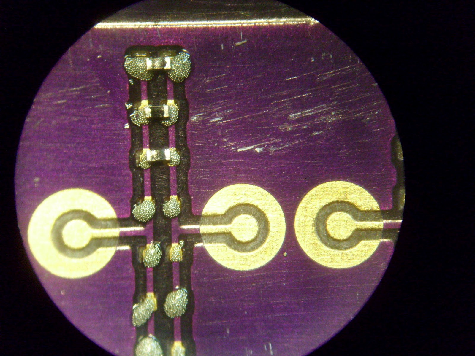
| Darkfield image of placed components before reflow. Focal plane is just above the top of the solder mask. |
I ran the board through my standard reflow profile in the toaster oven and let it cool. From a quick inspection it looked pretty good - no tombstoning or obvious shorts/opens.
This was confirmed with an ohmmeter check - 2.50KΩ exactly. Looks like a complete success :)
 |
| Board post-reflow. Note probe scrub marks on test pads. |
 |
| Darkfield closeup of a single component. Slight misalignment is visible on the one at the top edge, but electrical test passes. |
 |
| Assembled board seen next to an 14-pin PDIP for scale. |
It was a rather labor intensive process but the end result was a complete success. While I certainly am not about to go and use all 01005 components on my future boards, if it becomes necessary to stick something in a tight place it's good to know my process can handle it.


Hi Andrew
ReplyDeleteJust want to give you a vote of encouragement. Really enjoy reading your blog. I've caught the smaller bug but stopped at 0804 which are still easy to hand solder.
Lately I've been looking at the Omnivision CameraCube CMOS sensor. It's a 2.5mm package with a 4 x 5 BGA. Approximately a 0.6mm pitch.
With 4mil traces it seems just barely doable for the home hobbyist. Any thoughts?
Anyway, keep up the good work. Cheers.
Routing the outer row of balls on any BGA is trivial, and the next row in can be done without vias. If you can fit 4 mil traces between balls then you should be good as far as board fab goes (though 4 mil traces aren't exactly cheap...)
ReplyDeleteI have managed to solder 0.5mm BGAs (CPG56 package from Xilinx). My first two attempts were misaligned and the third worked well. You'll need to be very careful positioning the device but it should work out OK.
I suggest getting a cheap component of similar pitch and doing some process development tests first. Xilinx CoolRunner-II CPLDs in CPG56 package are relatively cheap (a dollar or two each) and thus would be good for practicing on. All you need is a JTAG programmer to verify that they were soldered properly.