Showing posts with label Thesis. Show all posts

Tuesday, October 1, 2013

SoC framework, part 5: JtagDebugController and nocswitch

All of the JTAG utilities I've been mentioning are quite handy if you need to load a bitstream onto a board from one of several workstations. But JTAG is capable of much more, including powerful on-chip debug features.

One of the often-overlooked hard IP blocks in Xilinx FPGAs is BSCAN. This primitive (usually described in the FPGA's configuration user guide) connects a JTAG data register for certain special instructions to FPGA fabric.

Xilinx 6 and 7 series FPGAs each contain four BSCANs, one connected to each of the four JTAG instructions USER1...USER4. These are very rarely used by user designs, but Xilinx utilities like ChipScope and the in-system SPI programming cores use them to communicate with the FPGA without needing additional connections.

The primitive is named BSCAN_SPARTAN6 in Spartan-6 and BSCANE2 in 7 series. As far as I can tell, both are functionally equivalent.


BSCAN_SPARTAN6 #(
 .JTAG_CHAIN(1)
)
user1_bscan (
 .SEL(instruction_active),
 .TCK(tck),
 .CAPTURE(state_capture_dr),
 .RESET(state_reset),
 .RUNTEST(state_runtest),
 .SHIFT(state_shift_dr),
 .UPDATE(state_update_dr),
 .DRCK(tck_gated),
 .TMS(tms),
 .TDI(tdi),
 .TDO(tdo)
);

The JTAG_CHAIN parameter specifies which of the four user instructions to use. I'll summarize the interesting ports below including some notes:
  • SEL goes high whenever USERx is loaded into the instruction register, regardless of the test state machine's current state.
  • CAPTURE, RESET, RUNTEST, SHIFT, UPDATE are one-hot flags that go high when the corresponding DR state is active. When the state machine is in the IR shift path, all flags are held low.
  • TMS is of little practical use since the state machine is already implemented for you.
  • TCK provides direct access to the JTAG clock. (Be sure to create a timing constraint for any signals clocked by this net.) In my experience the Xilinx tools often do not recognize this signal as a clock and use high-skew local routing; manual insertion of a BUFG/BUFH is advised for optimal results.
  • TDI and TDO are connected to the corresponding JTAG pins when in the SHIFT-DR state. You can connect any fabric logic you want to them.
Given this core plus libjtaghal on the PC side, we have a solid framework for building an on-chip debug system! The first step is to decide what sort of data to move over the link. Since my framework is NoC based, raw NoC frames seemed the natural choice. This would create a sort of layer-3 VPN encapsulating RPC/DMA transactions within JTAG scan operations.

After some experimenting with protocols I came up with one that seemed to work reasonably well. USER1 is the status/control register, USER2 is the RPC data register, and USER3 is the DMA data register. USER4 is left free for future expansion.

The FPGA side of the link is a module called JtagDebugController. It exposes RPC and DMA ports to the NoC; my current convention calls for addresses in subnet c000/2 to be routed to the debug bridge.

I'm deliberately not describing the actual on-wire protocol in depth because it's still in flux; when I get closer to a stable release I'll document it somewhere.

The PC side of the link is a C++ application using libjtaghal called "nocswitch". Example usage:

$./x86_64-linux-gnu/nocswitch --server localhost --port 50100 --lport 50101
Emulated NoC switch [SVN rev 1253:1254M] by Andrew D. Zonenberg.

License: 3-clause ("new" or "modified") BSD.
This is free software: you are free to change and redistribute it.
There is NO WARRANTY, to the extent permitted by law.

Connected to JTAG daemon at localhost:50100
Querying adapter...
    Remote JTAG adapter is a Dev board JTAG (232H) (serial number "FTWOON60", userid "FTWOON60", frequency 10.00 MHz)
Initializing chain...
Scan chain contains 1 devices
Device  0 is a Xilinx XC6SLX25 stepping 2
    Virtual TAP status register is  1000adba
    Valid NoC endpoint detected

This spawns a nocswitch listening on localhost:50101 connecting to a jtagd at localhost:50100.

Once nocswitch is running, it polls the status register on USER1 constantly waiting for the "new RPC message" or "new DMA message" bit to be set. (This causes a lot of traffic on the nocswitch-jtagd link and uses a decent amount of CPU on the host; my custom 8-port ICE will include FPGA based polling and an onboard nocswitch along with the jtagd's to avoid this problem.)

Client applications can then connect to nocswitch via a TCP-based protocol. The nocswitch assigns an address in c000/2 to each client in a manner somewhat reminiscent of DHCP; client applications (on the same machine or elsewhere on the LAN) can then send and receive NoC packets directly to the device under test. Multiple clients are fully supported; the nocswitch performs layer-2 switching between clients and the DUT as needed.

Nocswitch is able to switch frames from one client to another as well as just to the DUT; this permits a client to send messages to a NoC address without caring about whether it's a core in the SoC, a PC-side unit test, or even an RTL simulation (my mechanism for doing the latter will be described in a future post).

From a test case author's perspective, the NocSwitchInterface class implements the RPCAndDMAInterface class and supports the usual complement of operations.

printf("Connecting to nocswitch server...\n");
NOCSwitchInterface iface;
iface.Connect(server, port);

uint16_t eaddr = nameserver.ForwardLookup("eth0");
printf("eth0 is at %04x\n", eaddr);

printf("Resetting interface...\n");
iface.RPCFunctionCall(eaddr, ETH_RESET, 0, 0, 0, rxm);

Finally, here's a sneak peek at what's coming in future posts:
  • Hardware cosimulation, including a workaround for ISim's lack of Verilog PLI support
  • Splash, my build system inspired by Google Blaze
  • RED TIN, my internal logic analyzer (ChipScope/SignalTap replacement with lots of features useful in my work, like state machine decoding, RLE, and time-scale compression)
  • A look at both the hardware and software sides of the infrastructure for my dev board farm (batch scheduling, distributed build, automated testing, managed power distribution, and more). Hooking a single board up to a single JTAG dongle works fine if you only have one device but becomes a lot more of a pain to maintain when you have over twenty dev boards with more on the way!

Sunday, September 15, 2013

SoC framework, part 4: jtagd

As I mentioned in my previous post, libjtaghal supports a socket-based protocol for communicating with JTAG adapters. This allows some very powerful capabilities, for example sharing a single dev board among multiple developers.

The core of this is a TCP server written in C++ known as jtagd. So far I have tested it on Debian 7 on both x86_64-linux-gnu and arm-linux-gnueabihf architectures (laptop computer and Beaglebone Black).

The main jtagd executable connects to a JtagInterface object and bridges it out to a TCP socket using my custom protocol. The protocol is not 100% finalized at this point, several features (like a magic-number banner to verify the client is actually talking to a valid jtagd and not a mistyped port number) will be added before a public release.

Starting a jtagd is quite simple: run "jtagd --list" to see what interfaces are available, then connect to one of them.

azonenberg@mars$ jtagd --list
JTAG server daemon [SVN rev 1230M] by Andrew D. Zonenberg.

License: 3-clause ("new" or "modified") BSD.
This is free software: you are free to change and redistribute it.
There is NO WARRANTY, to the extent permitted by law.

Digilent API version: 2.9.3
    Enumerating interfaces... 2 found
    Interface 0: JtagSmt1
        Serial number:  SN:210203825011
        User ID:        JtagSmt1
        Default clock:  10.00 MHz
    Interface 1: JtagHs1
        Serial number:  SN:210205812611
        User ID:        JtagHs1
        Default clock:  10.00 MHz

FTDI API version: libftd2xx 1.1.4
    Enumerating interfaces... 16 found
    Interface 0: Digilent Adept USB Device A
        Serial number:  210203825011A
        User ID:        210203825011A
        Default clock:  10.00 MHz
   [[ Output trimmed for brevity ]]
    Interface 10: Dev Board JTAG
        Serial number:  FTWB6M0W
        User ID:        FTWB6M0W
        Default clock:  10.00 MHz
 
azonenberg@mars$ jtagd --api ftdi --serial 210203825011A --port 50200
JTAG server daemon [SVN rev 1230M] by Andrew D. Zonenberg.

License: 3-clause ("new" or "modified") BSD.
This is free software: you are free to change and redistribute it.
There is NO WARRANTY, to the extent permitted by law.

Connected to interface "Digilent Adept USB Device A (2232H)" (serial number "210203825011A")

Once the jtagd is running, you can connect to it using command-line tools such as jtagclient, or directly from C code using libjtaghal. The example here connects to a Digilent Atlys and verifies the device ID of the XC6SLX45 FPGA.

NetworkedJtagInterface iface;
iface.Connect(server, port);

//note use of RAII-style mutexing
//since jtagd is multi-client capable
JtagLock lock(m_iface);
m_iface->InitializeChain();

int ndev = m_iface->GetDeviceCount();
if(ndev == 0)
{
 throw JtagExceptionWrapper(
  "No devices found - invalid scan chain?",
  "",
  JtagException::EXCEPTION_TYPE_BOARD_FAULT);
}

//Verify that the board is an Atlys
//Should have a single XC6SLX45
XilinxSpartan6Device* pfpga = dynamic_cast<XilinxSpartan6Device*>(m_iface->GetDevice(0));
if(pfpga == NULL)
{
 throw JtagExceptionWrapper(
  "Device does not appear to be a Spartan-6",
  "",
  JtagException::EXCEPTION_TYPE_BOARD_FAULT);
}
if(pfpga->GetArraySize() != XilinxSpartan6Device::SPARTAN6_LX45)
{
 throw JtagExceptionWrapper(
  "Device is not an XC6SLX45",
  "",
  JtagException::EXCEPTION_TYPE_BOARD_FAULT);
}

The library internally uses low-level chain operations in order to talk to the device. The code below retrieves the "Device DNA" die serial number from a Spartan-6.

void XilinxSpartan6Device::GetSerialNumber(unsigned char* data)
{
 JtagLock lock(m_iface);
 
 Erase();
 
 //Enter ISC mode (wipes configuration)
 ResetToIdle();
 SetIR(INST_ISC_ENABLE);
 
 //Read the DNA value
 SetIR(INST_ISC_DNA);
 unsigned char zeros[8] = {0x00};
 ScanDR(zeros, data, 57);
 
 //Done
 SetIR(INST_ISC_DISABLE);
}

Stay tuned for my next post on nocswitch and the NoC-to-JTAG debug bridge :)

Saturday, September 14, 2013

SoC framework, part 3: libjtaghal

Almost all of my embedded development and debugging makes heavy use of JTAG, both for loading new bitstreams/firmware images and for interacting with on-chip debug systems.

When I first got into FPGA development I used the Xilinx Platform Cable USB II, which sells for $258.75 on Digikey as of this writing. It integrated nicely with the Xilinx IDE but I quickly grew frustrated. I wanted to use the BSCAN_SPARTAN6 primitive in the FPGA to move debug data on and off the FPGA using JTAG, but Xilinx does not provide any sort of API for scripting the platform cable. Although iMPACT allows manual bit twiddling in the chain as well as executing pre-made SVF files, there is no way to do interactive testing with it

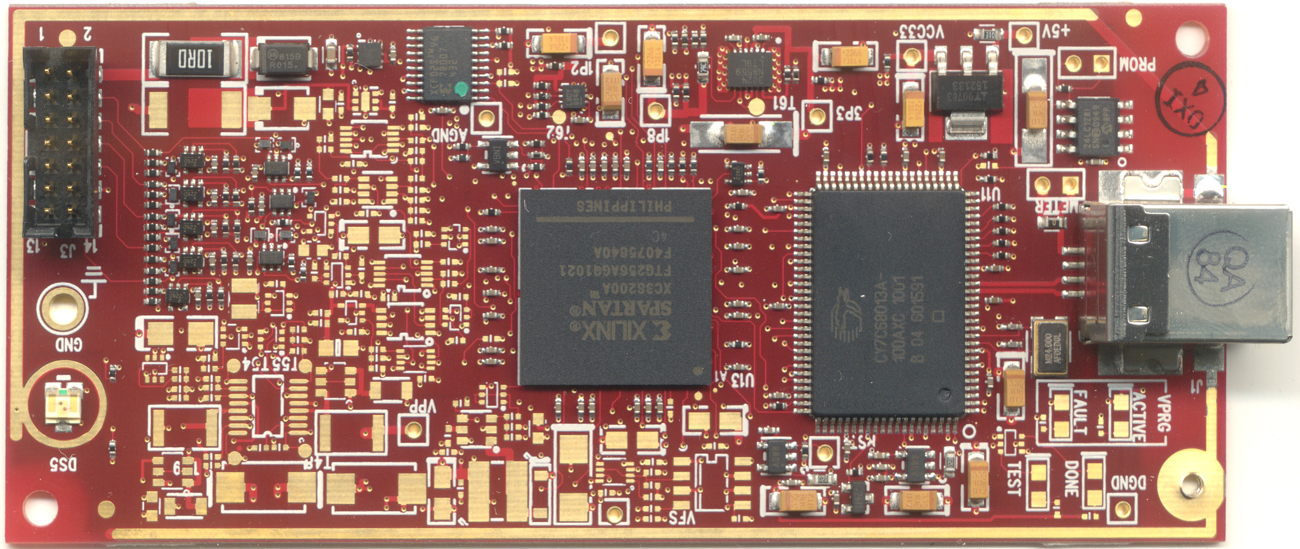
My first step in deciding how to proceed was to see what made their adapter tick. I would have opened up the adapter to see what was inside, but Bunnie saved me the trouble by posting pictures a while ago as the Name That Ware for March 2011.

Xilinx Platform Cable USB II (image courtesy of Bunnie)
The vast majority of the footprints on the board aren't even populated... one can only guess what additional functionality may have been planned at one point. There's an XC3S200A FPGA, a Cypress USB MCU, USB descriptor EEPROM, flash for the FPGA, and then a bunch of passives for power regulation and level shifting. Overall, the design is quite simple and certainly not worth $250.

After browsing for something cheaper and based on a well-known chipset, I found the Digilent HS1, a $54.99 FT2232-based adapter which is supported by Digilent's documented JTAG API and integrated nicely with the Xilinx IDE. In addition, since it's a standard FTDI chipset it would be possible to interact with it at a lower level using libftd2xx. (I also built a custom FT232H-based programmer that I have half a dozen of around my lab, but I wanted a known-good design to verify my software on first.)

The HS1 worked quite well using the Xilinx tools, but I still needed JTAG code to talk to it and interact with the FPGAs for scripted tests. I looked at a couple of popular options and rejected each of them:
  • OpenOCD (GNU GPL, incompatible with the BSD license used by my work)
  • xc3sprog (GPL, standalone tool with no API, includes programming algorithms that can run directly off a .bit file)
  • urjtag (GPL, has a socket-based JTAG server under development but not released yet)
It looked like I was going to have to write my own software, so I sat down and did just that. The result was a C++ library I call libjtaghal (JTAG hardware abstraction layer). It will be released publicly under the 3-clause BSD license once I've cleaned it up a bit; in the meantime if anyone wants a raw code drop with no documentation and a not-quite-finished build system leave a comment and I'll post something.

The basic structure of libjtaghal is built around two core object types: interfaces and devices. A JtagInterface represents a connection to a single JTAG adapter. As of now I support:
  • FT*232H MPSSE (assumes ADBUS7 is the output enable, an option to configure this is planned for the future)
  • Digilent API (for HS1 and integrated programmers on the Atlys etc)
  • Generic socket-based protocol for talking to remote libjtaghal servers
My custom 8-port JTAG system (more to follow in a future post) will use my socket-based protocol and show up as 8 separate interfaces which can each be controlled independently (potentially from 8 separate client PCs).

 A JtagDevice represents a single chip in a scan chain. Support for multi-device scan chains needs a bit more work; this is one of the reasons I haven't released it yet.

A given JtagDevice may implement one or more additional interfaces. Some of these are:
  • CPLD (generic complex programmable logic device)
  • FPGA (generic FPGA device)
  • ProgrammableDevice (any device which accepts firmware of some sort, including CPLDs, FPGAs, MCUs, and JTAG-capable ROMs)
  • RPCNetworkInterface (a device which supports sending RPC messages over JTAG)
  • DMANetworkInterface (a device which supports sending DMA messages over JTAG)
  • RPCAndDMANetworkInterface (implements RPCNetworkInterface, DMANetworkInterface, and some logic to connect the two protocols)
This design allows several very handy design abstractions. For example, the below code is the sum total of the "program" mode for my "jtagclient" command-line application. It takes a JtagInterface object "iface" and programs the device at chain index "devnum" with the firmware image "bitfile". Note the complete lack of any device- or interface-specific code. The same function can configure a CoolRunner-II via one of my custom FTDI programmers or a Spartan-6 using the integrated Digilent programmer on a dev board without changing anything.

JtagDevice* device = iface.GetDevice(devnum);
if(device == NULL)
{
 throw JtagExceptionWrapper(
  "Device is null, cannot continue",
  "",
  JtagException::EXCEPTION_TYPE_BOARD_FAULT);
}

//Make sure it's a programmable device
ProgrammableDevice* pdev = dynamic_cast(device);
if(pdev == NULL)
{
 throw JtagExceptionWrapper(
  "Device is not a programmable device, cannot continue",
  "",
  JtagException::EXCEPTION_TYPE_BOARD_FAULT);
}

//Load the firmware image and program the device
printf("Loading firmware image...\n");
FirmwareImage* img = pdev->LoadFirmwareImage(bitfile);
printf("Programming device...\n");
pdev->Program(img);
printf("Configuration successful\n");
delete img;

This is part of the test case for my gigabit Ethernet MAC, allocating a page of memory on the device under test by talking to the RAM controller at NoC address "raddr" via the RPCNetworkInterface "iface". (Details on how this is implemented will be coming in a few posts.)

printf("Allocating memory...\n");
iface.RPCFunctionCall(raddr, RAM_ALLOCATE, 0, 0, 0, rxm);
uint32_t txptr = rxm.data[1];
printf("    Transmit buffer is at 0x%08x\n", txptr);

There's a lot more to the system than this but I'll save the rest for my next post :)

Saturday, August 17, 2013

SoC framework, part 2: layer 2/3 protocols

Introduction

This is the second post in a series on the SoC framework I'm developing for my research. I'm going to get into more interesting topics (such as my build/test framework and FPGA cluster) shortly, but to understand how all of the parts communicate it's necessary to understand the basics of the SoC interconnect.

I'm omitting some of the details of link-layer flow control and congestion handling for now as it's not necessary to understand the higher-level concepts. If anyone really wants to know the dirty details, comment and I'll do a post on it at some point in the future.

As I mentioned briefly in part 1 of the series, my interconnect actually consists of two independent networks with the same topology. The RPC network is intended for control-plane transactions and supports function call/return semantics (request followed by response) as well as interrupts (one-way datagrams). The DMA network is meant for bulk data transfers between cores and memory devices.

Layer-2 header

The layer-2 header is the same for both networks:
31:2423:1615:87:0
Source addressDest address

This is then followed by the layer-3 header for the protocol of interest. Which protocol is in use depends on the interface; the routers are optimized for one or the other. I may consider changing this in the future.

DMA network

Packet format

31:2423:0
Layer-2 header
OpcodePayload length in words (only rightmost 10 bits implemented)
Physical memory address
Zero or more application-layer data words

Protocol description

The DMA network is meant for bulk data transfers and is normally memory mapped when used by a CPU.

It supports read and write transactions of an integer number of 32-bit words, up to 512 data words plus three header words. This size was chosen so that a DMA transfer could transport an entire Ethernet frame or typical NAND page in one packet.

Byte write enables are not supported; it is expected that a CPU core requiring this functionality will use read-modify-write semantics inside the L1 cache and then move words (or cache lines containing several words) over the DMA network.

The physical DMA address space is 48 bits: each of the 2^16 possible cores in the SoC has 32 bits of address space. If one core requires more than 4GB of address space it may respond to several consecutive DMA addresses. CPU cores are expected to translate the 48-bit physical addresses into 32 or 64 bit virtual addresses as required by their microarchitecture.

Write transactions are unidirectional: a single packet with opcode set to "write request" is all that is required. The destination host may send an RPC interrupt back on success or failure of the write however this is not required by the layer 3 protocol. Specific application layer APIs may mandate write acknowledgements.

Read transactions are bidirectional: a "read request" packet with length set to the desired read size, and no data words, is sent. The response is a "read data" packet with the appropriate length and data fields. As with write transactions, failure interrupts are optional at layer 3 but typically required by application layer APIs.

RPC network

Packet format

31:2423:2120:0
Layer-2 header
CallnumTypeApplication-layer data
Application-layer data

Protocol description

The RPC network is meant for small, low-latency control transfers and is normally register mapped when used by a CPU.

It supports fixed length packets of four word length so as to easily fit into standard register-based calling conventions.

The "callnum" field uniquely identifies the specific request / interrupt being performed. The meaning of this field is up to the application-layer protocol.

The "type" field can be one of the following:
  • Function call request
    The source host is requesting the destination host to perform some action. A response is required.
  • Function return (success)
    The source host has completed the requested action successfully. The application-layer protocol may specify a return value.
  • Function return (fail)
    The source host attempted the requested operation but could not complete it. The application-layer protocol may specify an error code.
  • Function return (retry)
    The source host is busy with a long-running operation and cannot complete the requested operation now, but might be able to in the future. The source host may re-send the request in the future or consider this to be a failure.
  • InterruptSomething interesting happened at the source host, and the destination host has previously requested to been notified when this happened.
  • Host prohibited
    Sent by a router to indicate that the destination host attempted to reach a host in violation of security policy. The source address of the packet is the prohibited address.
  • Host unreachable
    Sent by a router to indicate that the destination host attempted to reach a nonexistent address. The source address of the packet is the invalid address.

Monday, August 12, 2013

SoC framework, part 1: NoC overview and layer 1 structure

Those of you who have read my older posts may remember that I am currently pursuing a PhD in computer science at RPI. My research focus is the intersection of computer architecture and security, blurring classical distinctions between components in hopes of solving open problems in security. I'd go into more detail but I have to keep some surprises for my published papers ;)

As part of my research I am developing an FPGA-based SoC to test my theories. Existing frameworks and buses, such as AXI and Wishbone, lacked the flexibility I required so I had to create my own.

The first step was to forgo the classic shared-bus or crossbar topology in favor of a packet-switched network-on-chip (NoC). In order to keep the routing simple I elected to use a quadtree topology, with 16-bit routing addresses, for the network. This maps well to a spatially distributed system and should permit scaling to very large SoCs (up to 65536 IP cores per SoC are theoretically possible, though FPGA gate counts limit feasible designs to much smaller)

Example quadtree (from http://www.eecs.berkeley.edu/)
For the remainder of this post series I will use a slightly modified form of CIDR notation, as used with IP subnetting, to describe NoC addresses. For example, "8000/14" is the subnet with routing prefix 1000 0000 0000 00,  consisting of hexadecimal addresses 0x8000, 0x8001, 0x8002, and 0x8002. (Unlike IPv4 addressing, all addresses in the NoC are usable by hosts; there are no reserved broadcast addresses since all traffic is point to point.)

Each router has four downstream and one upstream ports. When a packet arrives at a router it checks if the packet is intended for its subnet; if so the next two bits control which downstream port it is forwarded out of. If the packet belongs to another subnet, it is sent out the upstream port.

Example NoC routing topology
As an example, if the host at 0x8001 wanted to send a message to the host at 0x8003, it would first reach the router for the 0x8000/14 subnet, The router checks the prefix, determines it to be a match, and then reads address bits 1:0 to determine that the packet should go out port 2'b11.

If 0x8001 were instead communicating with 0x8005, the router would instead forward the message out the upstream port. The router at 0x8000/12 would check address bits 3:2, determine that the packet is destined for port 2'b01, and forward to the destination router, which would then use bits 1:0 as the selector and forward out port 2'b01 to the final destination.

The actual network topology is slightly more complex than the diagram above implies, because my framework uses two independent networks, one for bulk data transfer and one for control-plane traffic. Thus, each line in the above diagram is actually four independent one-way links; two upstream and two downstream. Each link consists of a 32-bit data bus plus a few status bits. The actual protocol used will be described in the next post in this series.