Showing posts with label Teardowns. Show all posts

Monday, March 24, 2014

Microchip PIC32MZ process vs PIC32MX

Those of you keeping an eye on the MIPS microcontroller world have probably heard of Microchip's PIC32 series parts: MIPS32 CPU cores licensed from MIPS Technologies (bought by Imagination Technologies recently) paired with peripherals designed in-house by Microchip.
Although they're sold under the PIC brand name they have very little in common with the 8/16 bit PIC MCUs. They're fully pipelined processors with quite a bit of horsepower.

The PIC32MX family was the first to be introduced, back in 2009 or so. They're a MIPS M4K core at up to 80 MHz and max out at 128 KB of SRAM and 512 KB of NOR flash plus a fairly standard set of peripherals.

PIC32MX microcontroller

Somewhat disappointingly, the PIC32MX MMU is fixed mapping and there is no external bus interface. Although there is support for user/kernel privilege separation, all userspace code shares one address space. Another minor annoyance is that all PIC32MX parts run from a fixed 1.8V on-die LDO which normally cannot (the 300 series is an exception) be disabled or bypassed to run from an external supply.

The PIC32MZ series is just coming out now. They're so new, in fact that they show as "future product" on Microchip's website and you can only buy them on dev boards, although I'm told by around Q3-Q4 of this year they'll be reaching distributors. They fix a lot of the complaints I have with PIC32MX and add a hefty dose of speed: 200 MHz max CPU clock and an on-die L1 cache.

PIC32MZ microcontroller

On-chip memory in the PIC32MZ is increased to up to 512 KB of SRAM and a whopping 2 MB of flash in the largest part. The new CPU core has a fully programmable MMU and support for an external bus interface capable of addressing up to 16MB of off-chip address space.

I'm a hacker at heart, not just a developer, so I knew the minute I got one of these things I'd have to tear it down and see what made it tick. I looked around for a bit, found a $25 processor module on Digikey, and picked it up.

The board was pretty spartan, which was fine by me as I only wanted the chip.

PIC32MZ processor module
Less than an hour after the package had arrived, I had the chip desoldered and simmering away in a beaker of sulfuric acid. I had done a PIC32MX340F512H a few days previously to provide comparison shots.

Without further ado, here's the top metal shots:

PIC32MX340F512H
PIC32MZ2048ECH
These photos aren't to scale, the MZ is huge (about 31.9 mm2). By comparison the MX is around 20.

From an initial impression, we can see that although both run at the same core voltage (1.8V) the MZ is definitely a new, significantly smaller fab process. While the top layer of the MX is fine-pitch signal routing, the top layer of the MZ is (except in a few blocks which appear to contain analog circuitry) completely filled with power distribution routing.

Top layer closeups of MZ (left), MX (right), same scale

Thick power distribution wiring on the top layer is a hallmark of deep-submicron processes, 130 nm and below. Most 180 nm or larger devices have at least some signal routing on the top layer.

Looking at the mask revision markings gives a good hint as to the layer count and stack-up.

Mask rev markings on MZ (left), MX (right), same scale
The MZ appears to be one thick aluminum layer and five thin copper layers for a total of six, while the MX is four layers and probably all aluminum.

Enough with the top layer... time to get down! Both samples were etched with HF until all metal and poly was removed.

The first area of interest was the flash.

NOR flash on MZ (left), MX (right), different scales
Both arrays appear to be the same standard NOR structure, although the MZ's array is quite a bit denser: the bit cell pitch is 643 x 270 nm (0.173 μm2/bit) while the MX's is 1015 x 676 nm (0.686 μm2/bit). The 3.96x density increase suggests a roughly 2x process shrink.

The white cylinders littering the MX die are via plugs, most likely tungsten, left over after the HF etch. The MZ appears to use a copper damascene process without via plugs, although since no cross section was performed details of layer thicknesses etc are unavailable.

The next target was the SRAM.

6T SRAM on MZ (left), MX (right), different scales
Here we start to see significant differences. The MX uses a fairly textbook 6T "doughnut + H" SRAM structure while the MZ uses a more modern lithography-optimized pattern made of all straight lines with no angles, which is easier to etch. This kind of bit cell is common in leading-edge processes but this is the first time I've seen it in a commodity MCU.

Cell pitch for the MZ is 1345 x 747 nm (1.00 μm2/bit) while the MX is 1895 x 2550 nm (4.83 μm2/bit). This is a 4.83x increase in density.

The last area of interest was the standard cell array for the CPU.

Closeup of standard cells on MZ (left), MX (right), different scales
Channel length was measured at 125-130 nm for the MZ and 250-260 nm for the MX.

Both devices also had a significant number of dummy cells in the gate array, suggesting that the designs were routing-constrained.

Dummy cells in MZ
Dummy cells in MX

In conclusion, the PIC32MZ is a significantly more powerful 130 nm upgrade to the slower 250 nm PIC32MX family. If Microchip fixes most of the silicon bugs before they launch I'll definitely pick up a few and build some stuff with them.

I wasn't able to positively identify the fab either device was made on however the fill patterns and power distribution structure on the MZ are very similar of the TI AM1707 which is fabricated by TSMC so they're my first guess.

For more info and die pics check out the SiliconPr0n pages for the two chips:

Tuesday, February 4, 2014

Process overview: UMC 180nm eNVM

I've been reverse engineering a programmable logic device (Xilinx XC2C32A) made on UMC's 180nm eNVM process for the last few months and have been a little light on blog posts. I'm a big fan of the process writeups Chipworks does so I figured I'd try my hand at one ;)

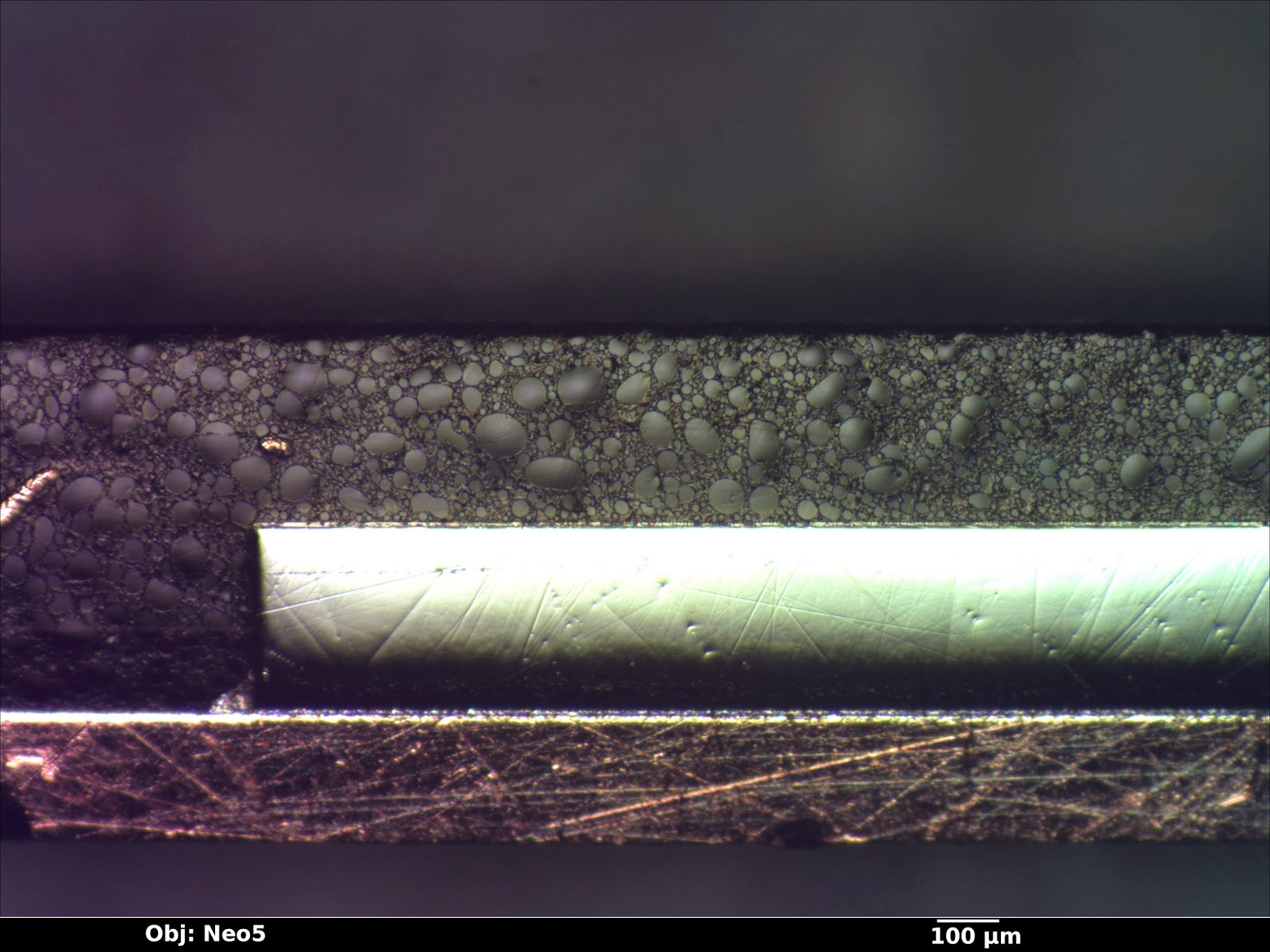
The target devices were packaged in a 32-pin QFN. The first part of the analysis was to sanding the entire package down to the middle of the device and polishing with diamond paste to get a quick overview of the die and packaging stack. (Shops with big budgets normally use X-ray systems for this.) There were a few scratches in the section from sanding, but since the closeups were going to be done on another die it wasn't necessary to polish them out.

Packaged device cross section

Total die thickness including BEOL was just over 300 μm. From the optical image, four layers of metal can be seen. The whitish color hinted that it was aluminum rather than copper, but there's no sense jumping to conclusions since the next die was about to hit the SEM.

A second specimen was depackaged using sulfuric acid, sputtered in platinum to reduce charging, and sectioned using a gallium ion FIB at a slight angle to the east-west routing.

FIB cross section of metal stack
From this image, it is easy to get some initial impressions of the process:
  • The overglass consists of two layers of slightly different compositions, possibly an oxide-nitride stack. 
  • The process is planarized up to metal 4, but not including overglass.
  • Metal has an adhesion/barrier layer at the top and bottom and not the sides, and is wider at the bottom than the top. This rules out damascene patterning and suggests that the metal layers are dry-etched aluminum.
  • Silicide layers are visible above the polysilicon gates and at the source/drain implants.
  • Vias have a much higher atomic number than the metal layers, probably tungsten.
  • Stacked vias are allowed and used frequently.
  • Well isolation is STI.
EDS spectra confirmed all these initial impressions to be correct.

M1 to M3 have pretty much identical stackups except for slight thickness differences: 100nm of Ti-based adhesion/barrier layer, 400-550 nm of aluminum conductor, then another barrier layer of similar composition. M4 is slightly thicker (850 nm aluminum) and the same barrier thickness.

The first overglass layer is the same material (silicon dioxide) as ILD; thickness ranges from slightly below the top of M4 to to 630 nm above the top. The second overglass layer has a slightly higher backscatter yield (EDIT: confirmed by EDS to be silicon nitride) and is about 945 nm thick.

M1-3 pitch is just over 600 nm, while the smallest observed M4 pitch is 1 μm.

EDS spectrum of wire on M4

A closer view of M3 shows the barrier metals in more detail. The barrier is a bit over 100 nm thick normally but thins to about 45 nm underneath upward-facing vias, suggesting that the ILD etch for drilling via holes also damages the barrier material. A small amount (around 30 nm) of sagging is present over the top of downward-facing vias.

Via sidewalls are coated with barrier metal as well, however it is significantly thinner (20 nm vs 100) than the metal layer barrier. The vias themselves are polycrystalline tungsten. Grain structure is clearly visible in the secondary electron image below.

(Note: The structure at left of the image is the edge of the FIB trench and stray material deposited by the ion beam and is not part of the actual device. The lower via is at a slight angle to the section so it was not entirely sliced open.)
M3 with upward/downward vias in cross section.
EDS spectrum of M1-M2 via area
The metal aspect ratio ranges from 3:1 on M1 to 1.5:1 on M4.

Now for the most interesting area - the transistors themselves!

The cross section was taken down the center of the CPLD's PLA OR array between two rows of 6T SRAM cells. Two PMOS transistors from each of two SRAM cells are visible in the closeup below.

Contacted gate pitch is 920 nm, for total cell width (including the 1180 nm of STI trench) of 2.9 μm. Plan view imaging shows total cell dimensions to be 2.9 x 3.3 μm or 9.5 μm2. This is a bit large for the 180 nm node and probably reflects the need to leave space on M1 and M2 for routing SRAM cell output to the programmable logic array.

SRAM cell structure and PLA AND array after metal/poly removal and Dash etch. (P-type implants are raised due to oxide growth from stain.)

Some variability in etch depth and sidewall slope is clearly visible on M1.

The polysilicon layer was hard to see in this view but is probably around 50 nm thick, topped by about 135 nm of cobalt silicide. (Gate oxide thickness isn't visible under SEM at the 180 nm node and I haven't yet had time to prepare a TEM sample.)

Source/drain contacts are made with a 70 nm thick cobalt silicide layer. All vias in the entire process appear to be about the same size (300 nm diameter) however the silicide contact pads are larger (465 nm).

Gate length is almost exactly 180 nm - measurement of the SEM image shows 175 nm +/- 12 nm.

Active area contacts and PMOS transistors
EDS spectrum of active-M1 contact
Closeup of PLA AND array after Dash etch showing PMOS and NMOS channels

Overall, the process seems fairly typical except for its use of aluminum for interconnect. It was a fun analysis and if I have time I may try to do a TEM cross section of both PMOS and NMOS transistors in the future. My main interest in the chip is netlist extraction, though, so this isn't a high priority.

I may also do a second post on the Flash portion of the chip.

EDIT: Decided to post a plan view SEM image of the flash array active area. This is after Dash etch; P-type areas have oxide grown over them. Poly has been stripped. The left-hand flash area is ten bits wide and stores configuration for function block 2's macrocells plus a "valid" bit. The right-hand area stores configuration for FB2's PLA (including both the AND and OR arrays, but not global routing).

Plan view SEM of flash
Finally, I would like to give special thanks to David Frey at the RPI cleanroom for assistance with the FIB cross section.

Sunday, July 15, 2012

MEMS pressure sensor teardown - part 2

The sensor I studied in my last post was delivered to me in a partially disassembled state. After returning to the e-waste dumpster we were able to find a fully intact unit.

SiliconPr0n wiki page: http://siliconpr0n.org/archive/doku.php?id=honeywell_awm2100v

The part number is clearly visible, it's a Honeywell AWM2100V airflow sensor. Some of my analysis from earlier was a bit off - it turns out that there's two ports on the device and some of the resistors on the membrane are heaters. One of the resistive elements is driven with a constant power and the resistance of the other one is measured to determine the membrane's temperature. Given the power input and the temperature increase above ambient (compared to unheated regions of the die and board) one can compute the airflow rate.

I tore this one down to the bare board but no further, die/board photos from the other unit are in part 1 of the post.

Sensor on the PCB
The original unit was a multi-board Honeywell process control module containing this sensor, a solenoid valve, and a large number of through-hole ICs including a Z88 family microprocessor (which may be covered in a future post - I want to get it decapped but haven't had time to do so yet).

I removed the sensor from the board using hot air. It's a six-pin SIL package with a plastic case snapped around the sensor board.


Packaging of sensor after removing from board

After removing the snapped-on casing we're left with the ceramic sensor board and a hose fitting on top. Under the host fitting is the actual sensor die, studied in detail in the previous post.

Fully disassembled

Saturday, July 14, 2012

MEMS pressure sensor teardown - part 1


While dumpster diving the e-waste bins on campus, one of my roommates found a control board of some sort that had an unusual sensor on it. We decided to take a closer look.

Sensor board
The board substrate is ceramic, most likely alumina. There are three electrically conductive layers visible on the board - gray (first level metalization), black (thick-film resistors), and gold (second level metalization and bond pads). A bluish dielectric separates M1 and M2 at crossing points but is not present over the remainder of the board.

The brownish reside on the top of the board is adhesive residue from the encapsulation over the sensor die.
Sensor die

The sensor die is approximately 1600μm along each side and appears to be made from a <100> oriented silicon wafer. Two metal layers are visible - one of a resistive material (most likely polysilicon) and one of gold (used for bond pads). For the sake of discussion I will define the upper center pin to be pin 1.

The die consists of six resistors and is entirely passive, with no transistors whatsoever.

The active sensing element consists of two membranes made out of what appears to be silicon nitride. The membranes are suspended over a cavity defined by an anisotropic wet etch using a KOH or related chemistry.

There are a total of three resistors between the membranes, whose values presumably change as the membrane is stressed. Pins 1 and 2, as well as 3 and 4, are connected to thin zigzag resistors on the left and right membranes respectively. Pins 7 and 8 connect to another resistor which starts on the lower left of the upper membrane, loops around at the far side, and goes back to the lower left on the lower membrane.

In addition, there are three resistors on the silicon substrate - betweens pins 8 and 9, 7 and 6, and 6 and 5. While they are all bonded out to pads and would be easy to measure, I have not yet attempted to get resistance readings.

The resistor between pins 5 and 6 has very unusual geometry and is not the typical zigzag I would expect. There is no obvious reason for this pattern.

Tuesday, July 3, 2012

Photobit PB-0100-5 teardown

Earlier today I was cleaning out a drawer in my lab and found a broken USB webcam. Before throwing it out I decided to desolder the sensor chip and have a look.

For those of you who aren't familiar with it, my friend John and I are the driving forces between the Silicon Pr0n project - a wiki dedicated to amassing knowledge about all things related to semiconductor RE. I haven't been doing as much work on it recently due to academic obligations but figured it was about time to post some more die photos!

Wiki page: http://siliconpr0n.org/archive/doku.php?id=azonenberg:photobit:pb0100

Map: http://siliconpr0n.org/map/photobit/pb-0100-5/neo5x/ 

Package shots after removing from the board:

Top view of sensor
Bottom view
The package is a ceramic LGA using gold ball bonding. I have so far made no attempt to remove the die from the package or delayer; all images were taken through the window on the front of the package.

Without even resorting to the microscope some structure is obvious:
  • The red and green area at the upper left of the die is the pixel array.
  • The remainder of the die is covered with a transparent blue material (which upon closer inspection looks exactly like the blue color filter in the pixels) to prevent photocurrents from messing up the control logic
  • The area below the sensor has a lot of fine detail and is irregular. It's probably an array of standard logic cells controlling the sensor readout.
  • The area to the right of the sensor looks very regular and is probably addressing logic, buffers, and the ADCs.
  • Several of the pins along the top and left edge have three bond wires instead of one. They're probably power/ground.
  • Not all bond pads are broken out to pins.
I made an imaging pass over the entire die with a 5x objective. Since I haven't had time to do a CNC mod on my microscope stage like John has, I have to move the stage and snap photos by hand. This makes high-magnification full-die imaging very time consuming so if I need that I'll usually send the chip to him for processing.

Without further ado here's the full-die image. Note that this is rotated 90 degrees clockwise from the package overview image so that the vendor logo is right side up.

Full-die image
Closer inspection reveals that the standard cell area at left has large spaces between rows of logic for interconnect, suggesting that this is a 2-metal design. As typical for 1999-era technology the metal layers are not planarized. Sub-pixels look to be about 5 μm across.

Random portion of the subpixel array
The bottom right of the die has the Photobit logo and copyright notice:

Vendor logo and copyright. Note probe scrub mark from wafer test on the upper right pad.
Right above the logo there were a bunch of ID markings from the individual masks. It's immediately obvious that several masks are not visible as there are gaps in the array. These are probably the implants.

Several metal layers are visible, along with at least one polysilicon and several whose purpose is not immediately obvious.

Mask ID markings
The most interesting feature observed was at the bottom left of the die - a little doodle of a panda bear snuck in by the layout engineer.

Mask art!

Thursday, March 3, 2011

Microchip PIC12F683 teardown

I'm going to kick off the meat of this blog with a teardown of a chip that has a special place in my memories - the first microcontroller I ever worked with, the Microchip PIC12F683. It's an 8-bit RISC microcontroller made on what looks like a 350nm 3-metal process, with 14 bit wide instructions and a fairly nice set of peripherals:
  • 2K words program Flash
  • 128 bytes SRAM
  • 256 bytes data EEPROM
  • Two 8-bit and one 16-bit timer
  • Four-channel multiplexed 10 bit A/D converter
  • Comparator
I decapped one of these a few months ago and imaged it at 400x magnification. Pin 1 is at the top left. (At the time I was still experimenting with panorama stitching techniques so there are a few alignment glitches.)

PIC12F683 metal 3 with passivation, magnified 400x

The glass layer (reddish) was quite annoying and made it hard to resolve traces so I decided to remove it using my standard wet-etch procedure (heating in 3% HF). I'll be writing about this process in more detail over the weekend.
PIC12F683 metal 3 after wet etching, magnified 400x
We now have enough information to create a floor plan of the chip:
  • The large block at bottom center (surrounded by power rails with 14 white capacitors at the bottom) is the program flash. Each capacitor is part of a charge pump used to generate high voltage for erasing one bit of flash.
  • Immediately to the left is the RAM.
  • Above the RAM is the EEPROM. As with the flash, there is one capacitor per bit of memory for high voltage generation.
  • Above the flash, and slightly to the right, are the configuration fuses. Each of the small red plates is part of a single configuration bit.
  • Analog peripherals are in an L-shape along the top and right sides
Top portion of PIC12F683 configuration fuse array (metal 3 after etching off glass)
The configuration fuses are single cells of EEPROM-style memory storing data such as the clock oscillator source and code / data protection bits. As with most other PICs, when the protection bit is in the "1" state the chip operates as normal; in the "0" state attempts to read firmware or EEPROM respectively via ICSP return all zeros. Configuration fuses can always be read.

EEPROM is typically susceptible to erasure (all bits set to 1) by strong UV light and the configuration fuses are no exception. If we can expose just the fuses (and not the flash or EEPROM, whose data we presumably want intact) to UV, the code protection can be removed and the firmware reverse-engineered using standard software RE tools. Note that PICs are thus a slightly easier target than Atmel chips. Atmel fuses in the "1" state indicates the chip is in the locked state (i.e. UV will set rather than clear the fuse).

Enough talking, time to try pwning the chip! As of this writing my decapping lab is offline, but Brooke Hill from Jimnson Research was kind enough to decap a few samples I sent him.
Decapped PIC12F683, magnified 10x. Rotated 90 degrees counterclockwise from other photos.
The first step was to plug the chip into a breadboard and verify it still worked. (Although decapping is normally a fairly low-risk procedure, bond wires do occasionally work loose during the rinse or cleaning steps.) The test firmware I used was a short piece of assembly that blinked an LED on GP2, and had the code-protection bit set.

I then laid down a mask over the memory areas I wanted to protect. I used the old classic, black nail polish applied with a lint-free swab under a stereo microscope. The brand of polish I purchased turned out to be very thick and gooey; in the future I intend to thin it with acetone for a more even coating.

Halfway through applying the mask
At this point the difficult work was over. I placed the chip inside my homemade UV erasure box, powered by two germicidal fluorescent bulbs.
UV exposure system
Two hours later the PIC was removed from UV and put back in the breadboard. I attempted to verify memory integrity with my PICKit 2.
Success! Program memory and EEPROM are undamaged (and unprotected) while configuration fuses read as all 1s.

Although the code protection on the PIC12F683 is clearly broken I am not finished with it; as an educational subject has not outlived its usefulness. Stay tuned for a future post with gate- and transistor-level analysis of interesting areas!