I've gotten a lot of requests recently to share some details on my BGA assembly process, so without further ado here it is!
The board in this example is a test vehicle with an 11x11 0.8mm XBGA footprint on it, being mounted with a PIC32MX engineering sample chip. This is the same board I used in my
0201 process test.
I deliberately put several unfilled vias in the pads to demonstrate why this is a bad idea. Keep reading for details!
 |
| 0.8mm XBGA test vehicle. Black marker lines highlight the row of balls that will be used for the cross section. |
Since I don't have in-house stencil capabilities and haven't gotten around to ordering professionally made ones, I do all of my BGAs with flux only. My preferred flux for this purpose is ChipQuik SMD291NL no-clean rosin tack flux.
 |
| BGA pads covered in flux |
The next step is to position the BGA on top of the footprint. Well-made footprints (such as the 256-FTBGA that I use on most of my FPGA boards) have the silkscreen outline slightly larger than the chip. Unfortunately this one is the same size as the chip so it was very difficult to align properly. I tried my best but it was still a little off.
 |
| BGA on footprint |
I then ran the board through the standard reflow profile in my toaster oven. It's a cheap Proctor-Silex oven purchased at WalMart for something like $25. There is no thermocouple or feedback circuit in it (I have a 120VAC rated relay and a thermocouple but have not hooked it up yet.)
- Set to 90C for 3 minutes to preheat
- Set to 150C for 1 minute for thermal soak.
- Set to 210C for 1 minute for reflow. This results in a Tal of about 15 seconds.
- Turn off oven, open door, and cool to ambient with room air
Note that these numbers are
not intended to describe the actual temperatures reached by the board or the oven - they're just the numbers on the dial of my specific oven. I know for a fact that the peak temperature reached at the 210C setting is in excess of 220C because that's the melting point of SAC305 solder.
I've also heard of people using oven thermometers to calibrate their reflow ovens. One word of caution for those doing this - if your sensor has a significantly higher thermal mass than your board (such as a big metal oven thermometer) its temperature will lag behind that of the less-massive PCB by a significant amount. I know of at least one hobbyist who reached the thermal decomposition point of FR4 Tg170 (somewhere around 300C) when his thermometer showed only 260!
The best way to tell when reflow is complete on an un-calibrated oven like mine is to watch the solder melt. My paste changes from a glossy gray (full of volatile flux compounds) to matte gray (once most of the flux has boiled off) to shiny silver (after the solder melts); BGA balls turn from a dull metallic color to shiny silver at melting; the chip also sinks slightly as the balls flatten from the weight of the IC.
This YouTube video (not from my lab) shows what a properly reflowing BGA looks like.
 |
| The test vehicle in the oven. Note scrap-grade 4-inch silicon wafer being used as "cookie sheet". |
Since this was a test board with no actual circuitry on it, the next step was to prepare to cross-section it and look at how well the joints turned out.
Although the flux I used is no-clean (and I normally leave it in place on most of my boards) cross sections look nicer if there isn't *too* much flux in the way. Since I don't have an ultrasonic cleaner yet (I do plan to buy one in the near future) I just let it soak in a beaker of 70% isopropyl alcohol for a few minutes, shook around a bit, and wiped it dry.
 |
| PCB sitting in beaker of IPA in my fume hood. Although IPA isn't particularly dangerous as solvents go, I have a general policy of keeping all open solvent containers in the hood whenever possible. |
Once the board was dry I cut it in half between the black lines with a Dremel and a cut-off wheel. My ShopVac-based dust control system works reasonably well, but I want to get a HEPA vac for this in the future.
After the rough cut I polished with 1200 grit sandpaper and wiped away the dust with a wet cloth. Upon looking under the microscope I saw that the failure I was hoping to demonstrate had indeed occurred - one of the balls had been sucked down into an uncapped via by capillary action, resulting in a complete lack of electrical contact. The ball at far right had been partially sucked into the via but the solder mask dam was big enough to keep it from going in all the way.
 |
| Cross section of PCB and BGA. Note solder-filled via in center and missing ball. The far-right via annular ring seems to have snagged on something during the cutting process and been ripped up off the board. |
Looking to one side of the board it was clear that the balls without vias under them had reflowed properly and were reasonably well aligned.
The black material between the balls is not underfill, it's a paste-like material made of residual flux, FR4/molding compound dust, and little slivers of copper that were ground off by the sanding process. It looks like my defluxing process didn't work as well as I had hoped; I'm going to need ultrasound to do the job properly.
One very interesting and unexpected result was visible in this cross section - the next row of vias were visible
through the FR4 laminate.
 |
| Three well-reflowed balls. Note vias in next row visible through laminate. |
Before closing up the lab for the night I decided to take one last picture to show what an ENIG-finished via looks like. Since this was a higher magnification image I followed the sandpaper polish with 3μm diamond paste to get a better finish.
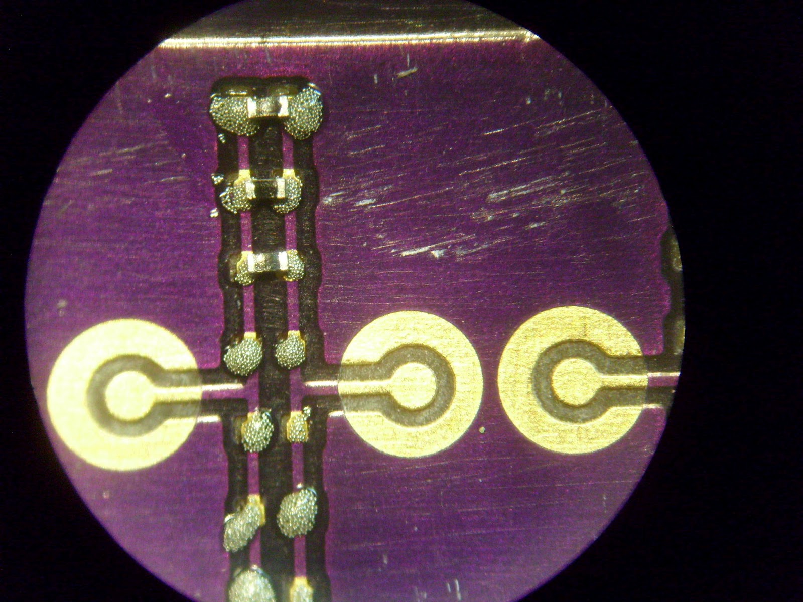
The layers visible in this image from bottom to top are FR4 (grayish), 1oz/35μm copper foil(copper) and what looks like about 10μm of nickel (yellow-gray). The gold plating is too thin to see at this magnification.
 |
| Cross section of ENIG-finished via. |