Showing posts with label Debugging. Show all posts

Sunday, February 5, 2017

STARSHIPRAIDER: Input buffer rev 0.1 design and characterization

Working as an embedded systems pentester is a lot of fun, but it comes with some annoying problems. There's so many tools that I can never seem to find the right one. Need to talk to a 3.3V UART? I almost invariably have an FTDI cable configured for 5 or 1.8V on my desk instead. Need to dump a 1.8V flash chip? Most of our flash dumpers won't run below 3.3. Need to sniff a high-speed bus? Most of the Saleae Logic analyzers floating around the lab are too slow to keep up with fast signals, and the nice oscilloscopes don't have a lot of channels. And everyone's favorite jack-of-all-trades tool, the Bus Pirate, is infamous for being slow.

As someone with no shortage of virtual razors, I decided that this yak needed to be shaved! The result was an ongoing project I call STARSHIPRAIDER. There will be more posts on the project in the coming months so stay tuned!

The first step was to decide on a series of requirements for the project:
  • 32 bidirectional I/O ports split into four 8-pin banks.
    This is enough to sniff any commonly encountered embedded bus other than DRAM. Multiple banks are needed to support multiple voltage levels in the same target.
  • Full support for 1.2 to 5V logic levels.This is supposed to be a "Swiss Army knife" embedded systems debug/testing tool. This voltage range encompasses pretty much any signalling voltage commonly encountered in embedded devices.
  • Tolerance to +/- 12V DC levels.Test equipment needs to handle some level of abuse. When you're reverse engineering a board it's easy to hook up ground to the wrong signal, probe a power rail, or even do both at once. The device doesn't have to function in this state (shutting down for protection is OK) but needs to not suffer permanent damage. It's also OK if the protection doesn't handle AC sources - the odds of accidentally connecting a piece of digital test equipment to a big RF power amplifier are low enough that I'm not worried.
  • 500 Mbps input/output rate for each pin.This was a somewhat arbitrary choice, but preliminary math indicated it was feasible. I wanted something significantly faster than existing tools in the class.
  • Ethernet-based interface to host PC.I've become a huge fan of Ethernet and IPv6 as communications interface for my projects. It doesn't require any royalties or license fees, scales from 10 Mbps to >10 Gbps and supports bridging between different link speeds, supports multi-master topologies, and can be bridged over a WAN or VPN. USB and PCIe, the two main alternatives, can do few if any of these.
  • Large data buffer.Most USB logic analyzers have very high peak capture rates, but the back-haul interface to the host PC can't keep up with extended captures at high speed. Commodity DRAM is so cheap that there's no reason to not stick a whole SODIMM of DDR3 in the instrument to provide an extremely deep capture buffer.
  • Multiple virtual instruments connected to a crossbar.Any nontrivial embedded device contains multiple buses of interest to a reverse engineer. STARSHIPRAIDER needs to be able to connect to several at once (on arbitrary pins), bridge them out to separate TCP ports, and allow multiple testers to send test vectors to them independently.
The brain of the system will be fairly straightforward high-speed digital. It will be a 6-8 layer PCB with an Artix-7 FPGA in FGG484 package, a SODIMM socket for 4GB of DDR3 800, a KSZ9031 Gigabit Ethernet PHY, a TLK10232 10gbit Ethernet PHY, and a SFP+ cage, plus some sort of connector (most likely a Samtec Q-strip) for talking to the I/O subsystem on a separate board.

The challenging part of the design, from an architectural perspective, seemed to be the I/O buffer and input protection circuit, so I decided to prototype it first.

STARSHIPRAIDER v0.1 I/O buffer design

A block diagram of the initial buffer design is shown above. The output buffer will be discussed in a separate post once I've had a chance to test it; today we'll be focusing on the input stage (the top half of the diagram).

During normal operation, the protection relay is closed. The series resistor has insignificant resistance compared to the input impedance of the comparator (an ADCMP607), so it can be largely ignored. The comparator checks the input signal against a threshold (chosen appropriately for the I/O standard in use) and sends a differential signal to the host board for processing. But what if something goes wrong?

If the user accidentally connects the probe to a signal outside the acceptable voltage range, a Schottky diode connected to the +5V or ground rail will conduct and shunt the excess voltage safely into the power rails. The series resistor limits fault current to a safe level (below the diode's peak power rating). After a short time (about 150 µs with my current relay driver), the protection relay opens and breaks the circuit.

The relay is controlled by a Silego GreenPAK4 mixed-signal FPGA, running a small design written in Verilog and compiled with my open-source toolchain. The code for the GreenPAK design is on Github.

All well and good in theory... but does it work? I built a characterization board containing a single I/O buffer and loaded with test points and probe connectors. You can grab the KiCAD files for this on Github as well. Here's a quick pic after assembly:

STARSHIPRAIDER I/O characterization board
Initial test results were not encouraging. Positive overvoltage spikes were clamped to +8V and negative spikes were clamped to -1V - well outside the -0.5 to +6V absolute max range of my comparator.
Positive transient response

Negative transient response


After a bit of review of the schematics, I found two errors. The "5V" ESD diode I was using to protect the high side had a poorly controlled Zener voltage and could clamp as high as 8V or 9V. The Schottky on the low side was able to survive my fault current but the forward voltage increased massively beyond the nominal value.

I reworked the board to replace the series resistor with a larger one (39 ohms) to reduce the maximum fault current, replaced the low-side Schottky with one that could handle more current, and replaced the Zener with an identical Schottky clamping to the +5V rail.

Testing this version gave much better results. There was still a small amount of ringing (less than five nanoseconds) a few hundred mV past the limit, but the comparator's ESD diodes should be able to safely dissipate this brief pulse.
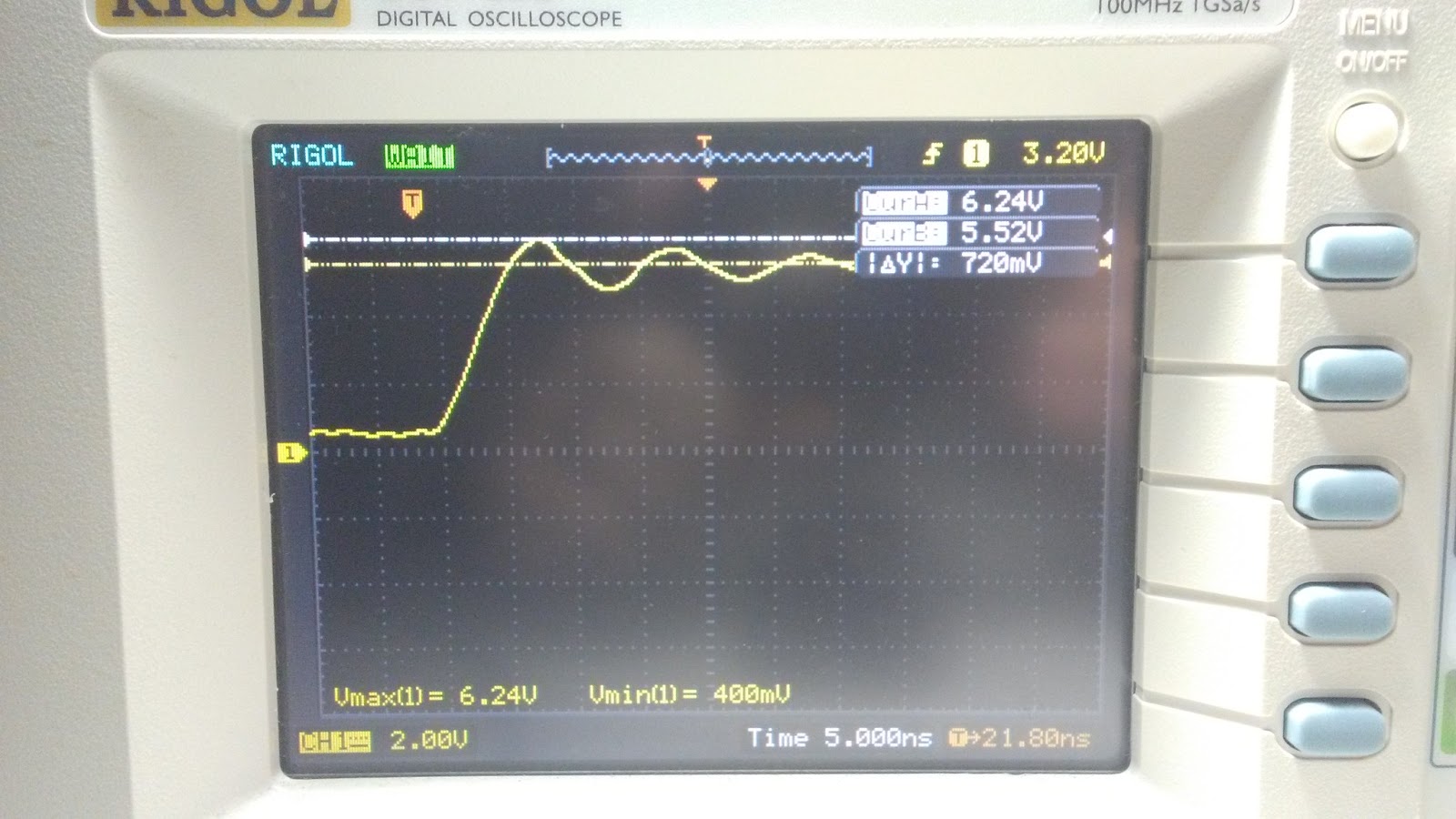
Positive transient response, after rework
Negative transient response, after rework
Now it was time to test the actual signal path. My first iteration of the test involved cobbling together a signal path from an FPGA board through the test platform and to the oscilloscope without any termination. The source of the signal was a BNC-to-minigrabber flying lead test clip! Needless to say, results were less than stellar.

PRBS31 eye at 80 Mbps through protection circuit with flying leads and no terminator
After ordering some proper RF test supplies (like an inline 50 ohm BNC terminator), I got much better signal quality. The eye was very sharp and clear at 100 Mbps. It was visibly rounded at 200 Mbps, but rendering a squarewave at that rate requires bandwith much higher than the 100 MHz of my oscilloscope so results were inconclusive.

PRBS31 eye at 100 Mbps through protection circuit with proper cabling
PRBS31 eye at 200 Mbps, limited by oscilloscope bandwidth
I then hooked the protection circuit up to the comparator to test the entire inbound signal chain. While the eye looked pretty good at 100 Mbps (plotting one leg of the differential since my scope was out of channels), at 200 Mbps horrible jitter appeared.

PRBS31 eye at 100 Mbps through full input buffer
PRBS31 eye at 200 Mbps through full input buffer
After quite a bit of scratching my head and fumbling with datasheets, I realized my oscilloscope was the problem by plotting the clock reference I was triggering on. The jitter was visible in this clock as well, suggesting that it was inherent in the oscilloscope's trigger circuit. This isn't too surprising considering I'm really pushing the limits of this scope - I need a better one to do this kind of testing properly.

PRBS31 eye at 200 Mbps plus 200 MHz sync clock
 At this point I've done about all of the input stage testing I can do with this oscilloscope. I'm going to try and rig up a BER tester on the FPGA so I can do PRBS loopback through the protection stage and comparator at higher speeds, then repeat for the output buffer and the protection run in the opposite direction.

I still have more work to do on the protection circuit as well... while it's fine at 100 Mbps, the 2x 10pF Schottky diode parasitic capacitance is seriously degrading my rise times (I calculated an RC filter -3dB point of around 200 MHz, so higher harmonics are being chopped off). I have some ideas on how I can cut this down much less but that will require a board respin and another blog post!

Friday, November 29, 2013

Bug hunting

This is the story of the hunt for a bug that I've been chasing, on and off, for the last month.

After my last post on the PDU, I began doing more exhaustive testing. I left Munin polling all of the stats every 5 minutes and kept the GUI open for maybe half an hour, turning channels on and off, and everything seemed fine...

Then I went away to do something else, came back to my desk, and saw that the GUI had frozen. The board wasn't responding to ping (or any network activity at all), and I had no idea why.

Other than confirming that the interconnect fabric was still working (by resolving the addresses of a few cores by the name server) there wasn't a ton I could do without adding some diagnostic code.

I then resynthesized the FPGA netlist with the gdb bridge enabled on the CPU. (The FPGA is packed pretty full; I don't leave the bridge in all the time because it substantially increases place-and-route runtime and sometimes requires decreasing the maximum clock rate). After waiting around half an hour for the build to complete I reloaded the FPGA with the new code, fired up the GUI, and went off to tidy up the lab.

After checking in a couple of times and not seeing a hang, I finally got it to crash a couple hours later. A quick inspection in gdb suggested that the CPU was executing instruction normally, had not segfaulted, and there was no sign of trouble. In each case the program counter was somewhere in RecvRPCMessage(), as would be expected when the message loop was otherwise idle. So what was the problem?

The next step was to remove the gdb bridge and insert a logic analyzer core. (As mentioned above the FPGA is filled to capacity and it's not possible to use both at the same time without removing application logic.)

After another multi-hour build-and-wait-for-hang cycle, I managed to figure out that the CPU was popping the inbound-message FIFO correctly and seemed to be still executing instructions. None of the error flags were set.

I thought for a while and decided to check the free-memory-page counter in the allocator. A few hours later, I saw that the free-page count was zero... a telltale sign of a memory leak.

I wasted untold hours and many rebuild cycles trying to find the source of the leak before sniffing the RPC link between the CPU and the network. As soon as I saw packets arriving and not being sent, I knew that the leak wasn't the problem. It was just another symptom. The CPU was getting stuck somewhere and never processing new Ethernet frames; as soon as enough frames had arrived to fill all memory then all processing halted.

Unfortunately, at this point I still had no idea what was causing the bug. I could reliably trigger the logic analyzer after the bug had happened and the CPU was busy-waiting (by triggering when free_page_count hit 1 or 0) but had no way to tell what led up to it.

RPC packet captures taken after the fault condition showed that the new-frame messages from the Ethernet MAC were arriving to the CPU just fine. The CPU could be clearly seen popping them from the hardware FIFO and storing them in memory immediately.

Eventually, I figured out just what looked funny about the RPC captures: the CPU was receiving RPC messages, issuing memory reads and writes, but never sending any RPC messages whatsoever. This started to give me a hint as to what was happening.

I took a closer look at the execution traces and found that the CPU was sitting in a RecvRPCMessage() call until a message showed up, then PushInterrupt()ing the message and returning to the start of the loop.

/**
 @brief Performs a function call through the RPC network.
 
 @param addr  Address of target node
 @param callnum The RPC function to call
 @param d0  First argument (only low 21 bits valid)
 @param d1  Second argument
 @param d2  Third argument
 @param retval Return value of the function
 
 @return zero on success, -1 on failure
 */
int __attribute__ ((section (".romlibs"))) RPCFunctionCall(
 unsigned int addr, 
 unsigned int callnum,
 unsigned int d0,
 unsigned int d1,
 unsigned int d2,
 RPCMessage_t* retval)
{
 //Send the query
 RPCMessage_t msg;
 msg.from = 0;
 msg.to = addr;
 msg.type = RPC_TYPE_CALL;
 msg.callnum = callnum;
 msg.data[0] = d0;
 msg.data[1] = d1;
 msg.data[2] = d2;
 SendRPCMessage(&msg);
 
 //Wait for a response
 while(1)
 {
  //Get the message
  RecvRPCMessage(retval);
  
  //Ignore anything not from the host of interest; save for future processing
  if(retval->from != addr)
  {
   //TODO: Support saving function calls / returns
   //TODO: Support out-of-order function call/return structures
   if(retval->type == RPC_TYPE_INTERRUPT)
    PushInterrupt(retval);
   continue;
  }
   
  //See what it is
  switch(retval->type)
  {
   //Send it again
   case RPC_TYPE_RETURN_RETRY:
    SendRPCMessage(&msg);
    break;
    
   //Fail
   case RPC_TYPE_RETURN_FAIL:
    return -1;
    
   //Success, we're done
   case RPC_TYPE_RETURN_SUCCESS:
    return 0;
    
   //We're not ready for interrupts, save them
   case RPC_TYPE_INTERRUPT:
    PushInterrupt(retval);
    break;
    
   default:
    break;
  }

 }
}

I spent most of a day repeatedly running the board until it hung to collect a sampling of different failures. A pattern started to emerge: addr was always 0x8003, the peripheral controller. This module contains a couple of peripherals that weren't big enough to justify the overhead of a full RPC router port on their own:
  • One ten-signal bidirectional GPIO port (debug/status LEDs plus a few reserved for future expansion)
  • One 32-bit timer with interrupt on overflow (used for polling environmental sensors for fault conditions, as well as socket timeouts)
  • One I2C master port (for talking to the DACs)
  • Three SPI master ports (for talking to the ADCs)
The two most common values for callnum in the hang state were PERIPH_SPI_SEND_BYTE and PERIPH_SPI_RECV_BYTE, but I saw a PERIPH_SPI_DEASSERT_CS call once. The GPIO and I2C peripherals aren't used during normal activity and are only touched when someone changes a breaker's trip point or the network link flaps, so I wasn't sure if the hang was SPI-specific or related to the peripheral controller in general.

After not seeing anything obviously amiss in the peripheral controller Verilog, I added one last bit of instrumentation: logging the last message successfully processed by the peripheral controller.

The next time the board froze, the CPU was in the middle of the first PERIPH_SPI_RECV_BYTE call in the function below (reading one channel of a MCP3204 quad ADC) but the peripheral controller was idle and had most recently processed the PERIPH_SPI_SEND_BYTE call on the line before.

unsigned int ADCRead(unsigned char spi_channel, unsigned char adc_channel)
{
 //Get the actual sensor reading
 RPCMessage_t rmsg;
 unsigned char opcode = 0x30;
 opcode |= (adc_channel << 1);
 opcode <<= 1;
 RPCFunctionCall(g_periphAddr, PERIPH_SPI_ASSERT_CS, 0,  spi_channel, 0, &rmsg);
 RPCFunctionCall(g_periphAddr, PERIPH_SPI_SEND_BYTE, opcode, spi_channel, 0, &rmsg); //Three dummy bits first
                      //then request read of CH0
                      //(single ended)
 RPCFunctionCall(g_periphAddr, PERIPH_SPI_RECV_BYTE, 0,   spi_channel, 0, &rmsg); //Read first 8 data bits
 unsigned int d0 = rmsg.data[0];
 RPCFunctionCall(g_periphAddr, PERIPH_SPI_RECV_BYTE, 0,  spi_channel, 0, &rmsg); //Read next 4 data bits
                      //followed by 4 garbage bits
 unsigned int d1 = rmsg.data[0];
 RPCFunctionCall(g_periphAddr, PERIPH_SPI_DEASSERT_CS, 0,  spi_channel, 0, &rmsg);
 
 return ((d0 << 4) & 0xFF0) | ( (d1 >> 4) & 0xF);
}

Operating under the assumption that my well-tested interconnect IP didn't have a bug that could make it drop packets randomly, the only remaining explanation was that the peripheral controller was occasionally ignoring an incoming RPC.

I took another look at the code and found the bug near the end of the main state machine:

//Wait for RPC transmits to finish
STATE_RPC_TXHOLD: begin
 if(rpc_fab_tx_done) begin
  rpc_fab_rx_done <= 1;
  state <= STATE_IDLE;
 end
end //end STATE_RPC_TXHOLD 

I was setting the "done" flag to pop the receive buffer every time I finished sending a message... without checking that I was sending it in response to another message. The only time this was ever untrue is when sending a timer overflow interrupt.

As a result, if a new message arrived at the peripheral controller between the start and end of sending the timer overflow message, it would be dropped. The window for doing this is only four clock cycles every 50ms, which explains the extreme rarity of the hang.

EDIT: Just out of curiosity I ran a few numbers to calculate the probability of a hang:
  • At the 30 MHz CPU speed I was using for testing, the odds of any single RPC transaction hanging are 1 in 375,000.
  • Reading each of the 12 ADC channels requires 5 SPI transactions, or 60 in total. The odds of at least one of these triggering a hang is 1 in 6250.
  • The client GUI polls at 4 Hz.
  • The chance of a hang occurring within the first 15 minutes of runtime is 43%.
  • The chance of a hang occurring within the first half hour is 68%.
  • There is about a 10% chance that the board will run for over an hour without hanging, and yet the bug is still there.

Wednesday, October 30, 2013

Desktop raised floor

It's been a while since I've posted about a project I've done rather than a tool or some of my reversing work. This one is purely mechanical too!

First, a little background. I have a lot of FPGA/CPLD/MCU dev boards on my desk. By "a lot" I don't mean two or three... more like 20. Powering this much hardware presents some interesting problems. I don't have that many USB ports (and many of them need more power than USB can provide). Wallwarts are another obvious solution, but I don't have enough outlets or wallwarts to power 20 boards either!

I made three bar-shaped USB hubs with male mini-B ports, to plug into small development boards backplane-style. This helped a bit, but as my collection of boards grew the situation got worse.

By last May, my desk looked something like this:

My desk full of cables
Despite extensive efforts to manage the cable disaster with split tubing, there was still a giant octopus. Worse yet, my power strips were full and half of my boards didn't even have power.

The first step was to replace the loose boards with a datacenter-style "raised floor". I bought a 2x3 foot sheet of clear blue acrylic from McMaster-Carr, carefully floorplanned where all of the boards would go, and then drilled holes for each board's mounting standoffs.

Drilling holes
This operation had to be done out on the kitchen table because my office was too small to work comfortably in.

Mounting USB hubs
I mounted all of the USB hubs to the underside of the board in order to save space on top for dev boards and things I was likely to need to probe. While this seemed a good idea at first, reaching underneath them to run cables was a little tricky. After finishing the build I replaced the legs with ones several inches longer to provide the necessary hand clearance.

Before running cables, I attached all of the boards and brought it back to my desk to test the fit.

The apparatus on my desk
The "hostnames" on labels below each board are used as node names for my batch scheduler and unit test framework (more on that in a future post). In addition, those boards with Ethernet interfaces are assigned a constant IP address by my DHCP server, recorded in DNS with that hostname so I can write test cases using hostnames instead of raw IP addresses.

In an effort to reduce cable mess, I made custom cut-to-size USB cables out of cat5 cable and soldered on USB plugs. This was a very slow and laborious process because the connectors tended to melt very easily no matter what temperature I ran the iron at. BGA is no problem for me but these connectors gave me a hard time; I had yields somewhere around 60-70% even after rework. The rest of the time the connectors were melted beyond repair.

Despite the pain, I think the results were worth it. I was a little worried about signal quality as USB is supposed to be 90 ohm Zdiff and cat5e is 100, but I've noticed no problems. I did try to find 90 ohm cables but had trouble locating any.

Custom USB cables
After running all of the cables I could, a few of the boards were still unpowered and there were wallwarts everywhere, but the data wiring was a bit neater. Definitely a step in the right direction, but more work was needed.
After initial deployment

After taking that picture, I replaced most of the red electrical tape with zip ties and stick-on mount points. This made the setup a lot neater but I don't have any photos of that handy.

In order to tidy it up properly, I needed to tackle the power problem. My solution to that is a bit of a long story so I'll save that for next post :)

Saturday, September 14, 2013

SoC framework, part 3: libjtaghal

Almost all of my embedded development and debugging makes heavy use of JTAG, both for loading new bitstreams/firmware images and for interacting with on-chip debug systems.

When I first got into FPGA development I used the Xilinx Platform Cable USB II, which sells for $258.75 on Digikey as of this writing. It integrated nicely with the Xilinx IDE but I quickly grew frustrated. I wanted to use the BSCAN_SPARTAN6 primitive in the FPGA to move debug data on and off the FPGA using JTAG, but Xilinx does not provide any sort of API for scripting the platform cable. Although iMPACT allows manual bit twiddling in the chain as well as executing pre-made SVF files, there is no way to do interactive testing with it

My first step in deciding how to proceed was to see what made their adapter tick. I would have opened up the adapter to see what was inside, but Bunnie saved me the trouble by posting pictures a while ago as the Name That Ware for March 2011.

Xilinx Platform Cable USB II (image courtesy of Bunnie)
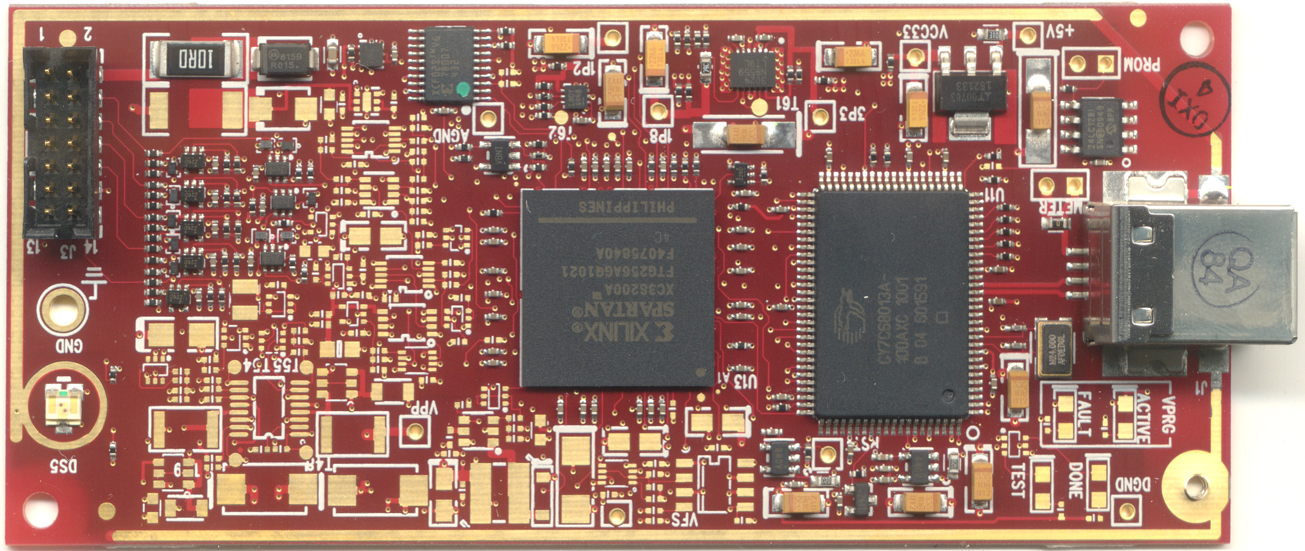
The vast majority of the footprints on the board aren't even populated... one can only guess what additional functionality may have been planned at one point. There's an XC3S200A FPGA, a Cypress USB MCU, USB descriptor EEPROM, flash for the FPGA, and then a bunch of passives for power regulation and level shifting. Overall, the design is quite simple and certainly not worth $250.

After browsing for something cheaper and based on a well-known chipset, I found the Digilent HS1, a $54.99 FT2232-based adapter which is supported by Digilent's documented JTAG API and integrated nicely with the Xilinx IDE. In addition, since it's a standard FTDI chipset it would be possible to interact with it at a lower level using libftd2xx. (I also built a custom FT232H-based programmer that I have half a dozen of around my lab, but I wanted a known-good design to verify my software on first.)

The HS1 worked quite well using the Xilinx tools, but I still needed JTAG code to talk to it and interact with the FPGAs for scripted tests. I looked at a couple of popular options and rejected each of them:
  • OpenOCD (GNU GPL, incompatible with the BSD license used by my work)
  • xc3sprog (GPL, standalone tool with no API, includes programming algorithms that can run directly off a .bit file)
  • urjtag (GPL, has a socket-based JTAG server under development but not released yet)
It looked like I was going to have to write my own software, so I sat down and did just that. The result was a C++ library I call libjtaghal (JTAG hardware abstraction layer). It will be released publicly under the 3-clause BSD license once I've cleaned it up a bit; in the meantime if anyone wants a raw code drop with no documentation and a not-quite-finished build system leave a comment and I'll post something.

The basic structure of libjtaghal is built around two core object types: interfaces and devices. A JtagInterface represents a connection to a single JTAG adapter. As of now I support:
  • FT*232H MPSSE (assumes ADBUS7 is the output enable, an option to configure this is planned for the future)
  • Digilent API (for HS1 and integrated programmers on the Atlys etc)
  • Generic socket-based protocol for talking to remote libjtaghal servers
My custom 8-port JTAG system (more to follow in a future post) will use my socket-based protocol and show up as 8 separate interfaces which can each be controlled independently (potentially from 8 separate client PCs).

 A JtagDevice represents a single chip in a scan chain. Support for multi-device scan chains needs a bit more work; this is one of the reasons I haven't released it yet.

A given JtagDevice may implement one or more additional interfaces. Some of these are:
  • CPLD (generic complex programmable logic device)
  • FPGA (generic FPGA device)
  • ProgrammableDevice (any device which accepts firmware of some sort, including CPLDs, FPGAs, MCUs, and JTAG-capable ROMs)
  • RPCNetworkInterface (a device which supports sending RPC messages over JTAG)
  • DMANetworkInterface (a device which supports sending DMA messages over JTAG)
  • RPCAndDMANetworkInterface (implements RPCNetworkInterface, DMANetworkInterface, and some logic to connect the two protocols)
This design allows several very handy design abstractions. For example, the below code is the sum total of the "program" mode for my "jtagclient" command-line application. It takes a JtagInterface object "iface" and programs the device at chain index "devnum" with the firmware image "bitfile". Note the complete lack of any device- or interface-specific code. The same function can configure a CoolRunner-II via one of my custom FTDI programmers or a Spartan-6 using the integrated Digilent programmer on a dev board without changing anything.

JtagDevice* device = iface.GetDevice(devnum);
if(device == NULL)
{
 throw JtagExceptionWrapper(
  "Device is null, cannot continue",
  "",
  JtagException::EXCEPTION_TYPE_BOARD_FAULT);
}

//Make sure it's a programmable device
ProgrammableDevice* pdev = dynamic_cast(device);
if(pdev == NULL)
{
 throw JtagExceptionWrapper(
  "Device is not a programmable device, cannot continue",
  "",
  JtagException::EXCEPTION_TYPE_BOARD_FAULT);
}

//Load the firmware image and program the device
printf("Loading firmware image...\n");
FirmwareImage* img = pdev->LoadFirmwareImage(bitfile);
printf("Programming device...\n");
pdev->Program(img);
printf("Configuration successful\n");
delete img;

This is part of the test case for my gigabit Ethernet MAC, allocating a page of memory on the device under test by talking to the RAM controller at NoC address "raddr" via the RPCNetworkInterface "iface". (Details on how this is implemented will be coming in a few posts.)

printf("Allocating memory...\n");
iface.RPCFunctionCall(raddr, RAM_ALLOCATE, 0, 0, 0, rxm);
uint32_t txptr = rxm.data[1];
printf("    Transmit buffer is at 0x%08x\n", txptr);

There's a lot more to the system than this but I'll save the rest for my next post :)

Friday, June 29, 2012

ISim bugs and introducing the RED TIN internal logic analyzer

Earlier this month I was working on a Spartan-6 based design using the on-chip DDR SDRAM controller (MCB) and ran into some problems.

For those of you not familiar with the MCB, it's a pipelined DDR/DDR2/DDR3 controller that exposes several (up to 2 full-duplex and 4 half-duplex, or 4 full-duplex) distinct ports to your RTL. Each port can be independently clocked and the order of operations between ports may be unpredictable due to this (a round-robin arbitration scheme is used under the hood after synchronization) but operations on a single port execute in FIFO order. My design only uses port 0 at the moment, 1/2/3 will probably be used for DMA at some point in the future.

Each port consists of three FIFOs, which are capable of independent clocking but in practice typically share the same clock:
  • Command FIFO, which specifies the address, opcode (read, write, read with auto precharge, write with auto precharge), and burst length (number of words to write)
  • Write data FIFO, which stores data to be written plus a byte write-enable mask
  • Read data FIFO, which stores data read from RAM
To issue a write, push one or more data words and masks onto the write data FIFO and then push a write command onto the command FIFO. To read, push a read command and then read from the read data FIFO as it becomes available.

The read and write FIFOs are each 128 words deep, enough to accommodate most needs. Unfortunately, the command FIFO is much shallower - 4 commands. 

In deeply pipelined designs that do a lot of random-access operations such as my softcore CPU this isn't nearly enough! It's only exacerbated by the poor performance of the quick-and-dirty direct-mapped write-through L1 cache I'm using (I plan to replace it with a 2-way set-associative write-back cache at some point).

The obvious fix was to put a bigger FIFO in front of the MCB. This didn't work for some reason and I found myself reading garbage from memory. It wasn't clear where the bug was from reading the code, so I tried to simulate my design in ISim and take a closer look.

Being a hobbyist operating on a grad student's stipend doesn't leave me a lot of cash to spend on software so I try to stick with open source, or at least freeware, tools to the extent possible. The >$3K-per-seat ISE Design Suite Logic Edition is obviously not affordable so I use the freeware ISE WebPack for all of my FPGA designs.

WebPack includes the "Lite Edition" of ISim instead of the full version. According to the ISim FAQ page:
There is only one limitation. When the user design + testbench exceeds 50,000 lines of HDL code, the simulator will start to derate the performance of the simulator for that invocation... The line count includes both testbench and source code lines. The Xilinx libraries are not included in the line count.

I figured I was fine... my line-count script showed 10,129 lines of Verilog in my design directory (not all of which was being used in the simulation) plus another ~15k in the generated MCB code - well below 50k. As soon as I fired up the simulator, though, it slowed to a crawl and displayed a nag screen in the console:
This is a limited version of the ISE Simulator. The current design has exceeded the design size limit for this version and the performance of the simulation will be derated. Please contact your nearest sales office at www.xilinx.com/company/contact.htm or visit the Xilinx on-line store at www.xilinx.com/onlinestore/design_resources.htm if interested in purchasing the full, unlimited version of this simulator.
A binary search of my RTL (commenting out half of the file at a time) revealed that the MCB primitive was causing the line count to be hit. Despite the FAQ claiming that the Xilinx libraries are not included in the count, the MCB's behavioral model clearly is included.

Since the derated simulation was unusably slow (the millisecond or two required for calibration to complete would have taken several days of wall-clock time, before even starting to simulate my test suite) this was clearly not a viable option.

I started to look around for alternatives. The DDR chip was being clocked at 80 MHz DDR'd to 160 MT/s, too fast for my 100 MHz oscilloscope/LA to be of any help. Since the RAM was dynamic I couldn't slow it down. I only had 20 GPIO channels on the board, not nearly enough to bring out all of the signals of interest for probing (not that this was really a problem as the LA only had 16 channels).

The best option at this point looked to be Xilinx's ChipScope internal logic analyzer, which supports programmable triggers and can store a large number (their documentation isn't clear on exactly how many) of channels of data to on-chip memory, then stream to a PC over JTAG or Ethernet (or possibly other IO standards too). Unfortunately ChipScope is not included in a license. My options were to spend $695 on a node-locked license, $850 on a floating license, or $3000+ on a full Logic Edition ISE license.

Not having that kind of cash, I realized I was out of easy options - I was going to have to write my own tool. I sat down and started coding on an internal logic analyzer of my own, dubbed RED TIN (two words picked randomly from a dictionary - I'm terrible at coming up with names!).

A week and 2,063 lines of code later I had an alpha version ready for testing at http://code.google.com/p/red-tin-logic-analyzer/. It consists of four parts:
  • RedTinLogicAnalyzer, a Verilog core which handles the core capture/buffering code (currently hard-coded to 128 channels and 512 samples, will be parameterizable later on).
  • RedTinUARTWrapper, a wrapper around RedTinLogicAnalyzer that implements the board-to-PC protocol (the intention is to eventually support JTAG and other interfaces as well).
  • The redtin application, a C++/gtkmm GUI application which functions as the control panel of the logic analyzer
  • A third-party waveform viewer that can read standard vcd-format files. gtkwave is hard-coded in the alpha build but I'll provide an interface for using other viewers later on.
The capture code is portable Verilog and should work on any FPGA, though I've only tested on Spartan-6. The PC-side application is cross-platform except for the UART code, which is Linux-specific (I haven't yet had time to write a portable wrapper around that).

Using the core is pretty simple - just insert it into the design, feed up to 128 inputs into the "din" input, supply a clock, and connect the UART pins up to top-level pins on the FPGA. Note the 50 bits of zeros at the end to pad the total width up to 128 bits.


Without further ado, here's a screenshot of it in action!


It's a little hard to see in the small view (I have a quad-monitor setup on my desk, this is the left half) but the left side shows the control panel application (with iMPACT in the background) and the right side is data captured from one of my boards.

After a bit of poking around I found my bug!

While I was pushing write commands onto the extended FIFO, I had somehow forgotten to do so with reads. This resulted in a race condition where reads could either be stepped on by writes or, even worse, occur before the write had committed!

The above screenshot shows a write (p0_cmd_instr = 3'b000) executing after a read (p0_cmd_instr = 3'b001) even though the write was issued first (compare rising edge of wr to rising edge of read_active). As a result the read data was complete garbage (32'hDFBDBFEF instead of 32'hFEEDFACE) because nothing had been written to that address yet.