Saturday, March 24, 2012

Analysis of RadioShack Duster Spray

In research and industry, spraying with compressed gas (usually dry nitrogen) is the standard way to remove liquid from a specimen after solvent cleaning or rinsing. By blowing the liquid off rather than letting it evaporate, spots from dissolved contamination are reduced or eliminated.

I had been using RadioShack duster spray for a while but started noticing residue on samples dried with it. My hypotheses at this point were:
  • The solvent had contamination in it, either from cleaning the sample or a contaminant in my stock bottle, and was depositing the contaminant on my samples
  • The bitterant added to the duster spray (to deter people from using it as an inhalant) was less volatile than the gas (or not volatile at all) and leaving residue on the samples

Earlier today I decided to test the spray and see if I could find out whether it was the source of the contaminant. Since the labeling on the can indicated pretty clearly that breathing it wasn't a great idea, all of my work was done in the fume hood.

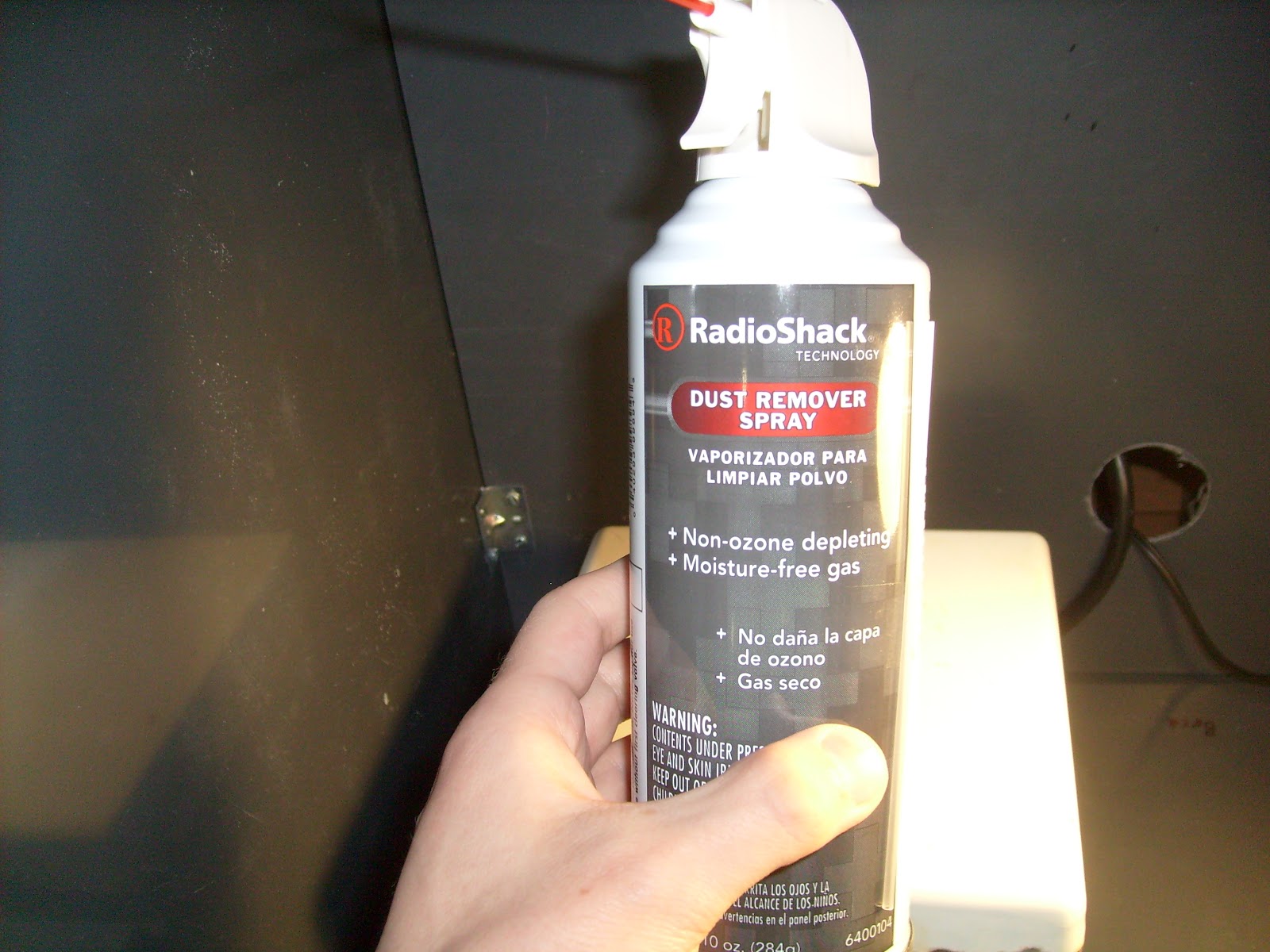
The subject of today's experiments


I began by inverting the can and spraying a liquefied sample of the duster (R-134A refrigerant, according to the label on the can) into a test tube. The tube was quickly coated in frost as the refrigerant evaporated.

Frost-covered test tube
After trying to place some of the liquid onto a microscope slide with little success (it boiled as soon as the pipette touched it) I ended up pouring it into a petri dish and leaving it on the hot plate to evaporate all of the refrigerant and condensed water.

R-134a and condensed water slush being evaporated on the hot plate
Non-volatile contamination deposited on petri dish
Non-volatile contamination deposited on microscope slide

The results were pretty conclusive - some non-volatile contaminant is definitely present in the spray. I'm not sure what it is, and see little point in trying to identify it, but I clearly need to find a new source of duster gas for my experiments.

I'm looking at CleanTex duster spray, from the vendors of Texwipe cleanroom wipers. According to the specs on the website it's particulate filtered down to 200nm and is pure compressed gas with no bitterant or other stuff added.

Saturday, January 14, 2012

First BGA board

(NOTE: This was originally scheduled to happen a lot earlier but the fab screwed up shipping on the boards. I only got them today.)

A while ago I decided to get serious about doing a design based on the Spartan-6 FPGA. Unfortunately all but the smallest part in the family are BGA only. They're somewhat pricey ($40ish for the XC6SLX25) so I figured it'd be a good idea to practice on something less expensive!

Quick calculations given the DorkbotPDX batch order's design rules showed that anything under 1mm pitch was not possible in a full array since a via could not fit between adjacent balls. This rules out the CPG196, CSG225, CSG324, and CSG484 packages. The remaining options are FTG256, FGG484, FGG676, and FGG900. FTG256 looked like the easiest as it had the least pins.

I did a bit of catalog browsing and determined that the cheapest FTG256 part available from Xilinx was the XC3S50A, which at $10 a pop was still a bit expensive for testing BGA soldering processes.

Eventually I settled on CPG56 packaged CoolRunner-II CPLDs as my first victim (Digikey page). CPG56 is 0.5mm pitch but is only two concentric rings, not full array.
CPG56 packaged CPLD


The next step was to design a board. I went with a simple 2-layer design that did not break out all of the balls, but seemed to offer enough IOs to be useful for casual testing.

Once the boards arrived I quickly inspected them under my microscope. They were the typical DorkbotPDX batch boards - purple LPI soldermask and ENIG finish on the pads. Some of the unbonded pads (A7-A9) appeared to have lifted off the board or underetched during manufacture. Since the pads weren't being used in the board layout this was not a problem, though it did mean the chip would be attached a bit less securely. I forgot to take a photo of this but will try to upload one soon.

I have a Proctor-Silex toaster oven I had used for reflow several times in the past but never on a BGA. There is no thermocouple or automatic temperature profile control on the oven yet (a Type-K thermocouple is inbound from Sparkfun as I write this) so I used my standard manual profile for lead-free solder, adjusting the thermostat by hand for each step:
  • Heat quickly from room temperature to just below 100C
  • Soak at 100C for 30-60 seconds
  • Ramp up to 180C, hold for 15-30 seconds
  • Ramp up to 220C, hold for 15 seconds
  • Open door, wait 30 seconds, remove board
The first two attempts at soldering failed as the chip was not even close to correctly aligned. The first (pic coming soon) was so far off (about 250 μm) that none of the balls even touched the pads. Visible holes in the flux residue showed just how far off center it had been. The second was slightly better but still not usable.

One of the first two reflow attempts
On the third attempt I paid extra attention to centering the chip and it seemed to turn out well. I then hand-soldered the clock oscillator, voltage regulator, JTAG header, and the 0402 sized decoupling capacitors on the back.

When I attempted to solder the breadboard headers I realized I had used the wrong drill size and the pins didn't fit. Since the only ones I really cared about were power and ground I just soldered two wires into the holes.

Finished board, top view
Finished board, bottom view
Electrical test showed no shorts anywhere between adjacent balls. Optical inspection looked good too.

Side view of CSBGA
After hooking it up to a 3.3V power rail and a JTAG programmer, I was able to successfully program it with a simple design (divide-by-2 counter). Oscilloscope confirmed a nice 10 MHz squarewave on the output when driven by 20.

Saturday, December 31, 2011

Multiple Lithography in Homemade PCBs

Earlier this week I decided it was about time to try making a board for some of the 24AA16 EEPROMs I had sampled from Microchip a year ago. It's a 16kbit I2C EEPROM with five pins: power, ground, I2C data and clock, and write protect.

Five pin package - piece of cake, right? But, just to add to the fun, the package I picked was CSBGA with balls about 250μm apart!

From the packaging specification, it can be seen that the balls are 150 μm diameter and spaced in a 2x2 grid 570μm x 520μm with one more in the center. This is a little smaller than my laser-printer contact lithography process can comfortably resolve. What to do?

Conveniently I have a metallurgical microscope that I've managed to coax into service as a projection lithography system. The field of view is, however, far too small to do an entire PCB.

After a little thinking I decided to try a multiple-exposure technique. The first step was to design a board layout in ExpressPCB (my preferred CAD tool is kicad but Express is a little easier for super simple layouts) with a 4-pin SIL header going to a rectangle of copper a little bigger than the CSP footprint. I also made a second mask containing the BGA footprint and tracks going out to four large pads, and printed it at 4x actual size. The center ball is WP# so I tied it to Vdd rather than breaking out to a separate pin.

Mask design

I then printed a mask on my printer, exposed onto precoated PCB, developed (1% w/v NaOH in distilled water), and etched (6 parts 3% H2O2 : 1 part 32% HCl at low heat) as with my standard PCB process.

The next step was to strip the existing photoresist since it had been exposed to light during the etch process. A few drops of acetone did the trick nicely.

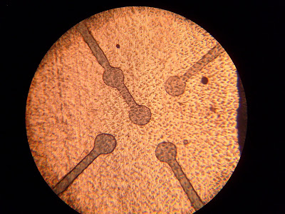
I then spin-coated the board with fresh photoresist, using my standard mixture (Shipley SP24 photoresist diluted 50% v/v with acetone for a thinner layer), soft baked on a hot plate, and exposed the BGA mask onto the copper rectangle. After developing, this was the result:

Second photomask on top of etched metal1

Closer view showing edge quality
Not surprisingly, the resolution and edge roughness were vastly better than the contact lithography process. (I've scaled the same technique to 20 μm half-pitch on silicon and there's room to go a lot further.) In retrospect the traces were a little too small considering that the copper layer they're sitting on is 35 μm thick, but this was a mask design error and not a process issue.

Since the thin photoresist I use is harder to see on copper than the thick stuff the board came coated with, I tossed it in the etchant for a couple of seconds to make it more obvious what was being masked.

After a couple seconds in the etch bath

The copper pad was also a bit larger than it needed to be and exceeded the FOV of the lithography system (note the unwanted photoresist shorting the pads together). I gently scraped this away with a #11 scalpel blade under 30x magnification and briefly etched to confirm good separation.

Surgery time!

After etching, no shorts

I then etched for a couple of minutes and removed the board to see how it was doing.

Almost done etching
Things still looked very good, all traces were intact. For traces with such a high aspect ratio (about 40 μm wide in 35 μm thick copper) things looked surprisingly good, but it needed a little more time.

Overetched. (photoresist stripped before taking this pic)
Unfortunately I overetched, one of the traces was gone entirely and another was seriously damaged. Some residue was still in place between two of the pads. Perhaps better agitation would help?

In either case, had the traces been a little larger (perhaps 75 μm) or the copper a little thinner it would have worked beautifully. The lithography itself was flawless and even though the board was not usable it appears the technique is feasible. Given a mask respin this same board could be fabricated with little difficulty.
Friday, December 30, 2011

SITREP - December 2011

Figured it's about time I posted an update since I haven't had time to write for a while, I just started the PhD program and my work has been keeping me busy.

I'm going to be broadening the focus of this blog a bit to cover topics besides reverse engineering: general electronics, FPGA design, semiconductor fabrication, infosec, and various other related stuff.

My focus will be on things generally considered too difficult for hobbyists, like BGA soldering and MEMS/CMOS fabrication.

Expect a series of posts over the next few days on my newly upgraded lab!

Wednesday, March 16, 2011

Wet delayering process

My preferred method for delayering chips is wet etching in dilute hydrofluoric acid (HF), commonly available in grocery stores as Whink brand rust remover:

~2% technical grade HF from Price Chopper
As the MSDS makes quite clear, this stuff is not something you want to splash on your hands (or skin in general). While it's extremely dilute compared to the 45% concentrated solution used in some laboratories, I've been through the HF safety talk at my school's cleanroom enough times that I'd rather not take chances.

I have a pair of Norfoil (Silver Shield) gloves around that I use for this kind of work. They're rather stiff so a common practice to improve dexterity is to double-glove with an XL nitrile glove over the Norfoil. When combined with a lab coat, splash goggles, and a face shield there's little chance of anything getting through. (EDIT: A fume hood is significantly safer; at the time of this post I didn't have one so I just tried to work with the smallest volume possible. I do now and wouldn't repeat the experiment outside it.)

 
Nitrile outer glove (blue) over Norfoil glove (silver), tucked into sleeve of Tyvek lab coat (white)

My standard lab PPE

Before getting dressed I placed a 10 ml beaker of distilled water on my hot plate and preheated it to a warm but not boiling temperature (exact temp isn't critical).

The next step is to pour a bit under 1 ml of the HF solution into a plastic test tube. HF will eat glass so using glass labware with it isn't a good idea!

HF solution in the test tube
Drop the die into the tube, cap it, and place it in the water bath. Etch rate depends on temperature, strength of the acid (Whink's strength isn't precisely controlled and I often will re-use the acid several times) and a few other factors so it's difficult to accurately predict. I usually will etch for 30 seconds at a time on modern planarized processes and 60-90 seconds on a large non-planarized chip.
Sample etching in the water bath

When the time is up, remove the tube from the heat and suction the HF with a pipette. The acid can usually be re-used for many etches, though it does get weaker over time. Drop the die into a beaker of acetone to remove any acid residue.

Remove the sample from the acetone using solvent-resistant plastic tweezers. (Many common plastics, such as polycarbonate, will dissolve into the acetone and contaminate your sample. Metal tweezers have a nasty habit of chipping edges of dies.)

Rapidly blow-dry the sample, holding it down with tweezers so it doesn't go flying. I used a can of R-134 duster spray. (If you let the solvent evaporate slowly large crystals can form from dissolved materials.)

Drying the sample
Image the die under a microscope to see if you've etched far enough. (The die I used in this demonstration was actually a bit over-etched as I paid more attention to camera angles than etch timing!)

The other main delayering method I plan to explore is CMP with colloidal silica. At the moment MTI is sold out, but when a new shipment arrives expect a post on CMP!


Thursday, March 3, 2011

Microchip PIC12F683 teardown

I'm going to kick off the meat of this blog with a teardown of a chip that has a special place in my memories - the first microcontroller I ever worked with, the Microchip PIC12F683. It's an 8-bit RISC microcontroller made on what looks like a 350nm 3-metal process, with 14 bit wide instructions and a fairly nice set of peripherals:
  • 2K words program Flash
  • 128 bytes SRAM
  • 256 bytes data EEPROM
  • Two 8-bit and one 16-bit timer
  • Four-channel multiplexed 10 bit A/D converter
  • Comparator
I decapped one of these a few months ago and imaged it at 400x magnification. Pin 1 is at the top left. (At the time I was still experimenting with panorama stitching techniques so there are a few alignment glitches.)

PIC12F683 metal 3 with passivation, magnified 400x

The glass layer (reddish) was quite annoying and made it hard to resolve traces so I decided to remove it using my standard wet-etch procedure (heating in 3% HF). I'll be writing about this process in more detail over the weekend.
PIC12F683 metal 3 after wet etching, magnified 400x
We now have enough information to create a floor plan of the chip:
  • The large block at bottom center (surrounded by power rails with 14 white capacitors at the bottom) is the program flash. Each capacitor is part of a charge pump used to generate high voltage for erasing one bit of flash.
  • Immediately to the left is the RAM.
  • Above the RAM is the EEPROM. As with the flash, there is one capacitor per bit of memory for high voltage generation.
  • Above the flash, and slightly to the right, are the configuration fuses. Each of the small red plates is part of a single configuration bit.
  • Analog peripherals are in an L-shape along the top and right sides
Top portion of PIC12F683 configuration fuse array (metal 3 after etching off glass)
The configuration fuses are single cells of EEPROM-style memory storing data such as the clock oscillator source and code / data protection bits. As with most other PICs, when the protection bit is in the "1" state the chip operates as normal; in the "0" state attempts to read firmware or EEPROM respectively via ICSP return all zeros. Configuration fuses can always be read.

EEPROM is typically susceptible to erasure (all bits set to 1) by strong UV light and the configuration fuses are no exception. If we can expose just the fuses (and not the flash or EEPROM, whose data we presumably want intact) to UV, the code protection can be removed and the firmware reverse-engineered using standard software RE tools. Note that PICs are thus a slightly easier target than Atmel chips. Atmel fuses in the "1" state indicates the chip is in the locked state (i.e. UV will set rather than clear the fuse).

Enough talking, time to try pwning the chip! As of this writing my decapping lab is offline, but Brooke Hill from Jimnson Research was kind enough to decap a few samples I sent him.
Decapped PIC12F683, magnified 10x. Rotated 90 degrees counterclockwise from other photos.
The first step was to plug the chip into a breadboard and verify it still worked. (Although decapping is normally a fairly low-risk procedure, bond wires do occasionally work loose during the rinse or cleaning steps.) The test firmware I used was a short piece of assembly that blinked an LED on GP2, and had the code-protection bit set.

I then laid down a mask over the memory areas I wanted to protect. I used the old classic, black nail polish applied with a lint-free swab under a stereo microscope. The brand of polish I purchased turned out to be very thick and gooey; in the future I intend to thin it with acetone for a more even coating.

Halfway through applying the mask
At this point the difficult work was over. I placed the chip inside my homemade UV erasure box, powered by two germicidal fluorescent bulbs.
UV exposure system
Two hours later the PIC was removed from UV and put back in the breadboard. I attempted to verify memory integrity with my PICKit 2.
Success! Program memory and EEPROM are undamaged (and unprotected) while configuration fuses read as all 1s.

Although the code protection on the PIC12F683 is clearly broken I am not finished with it; as an educational subject has not outlived its usefulness. Stay tuned for a future post with gate- and transistor-level analysis of interesting areas!

Welcome

Hello readers, and welcome to my virtual laboratory!

I am an undergraduate computer science student at Rensselaer Polytechnic Institute (beginning my PhD this the fall) with a wide variety of technical interests. The focus of this blog is my research into integrated circuit reverse engineering.

While many hardware reverse engineering blogs (such as that of Tarnovsky) are primarily focused with defeating configuration fuses and anti-tamper circuitry, I hope to cover a wide range of topics including these as well as general CMOS logic and sample preparation techniques.

For the skeptics among you, the right to reverse engineer ICs is protected by United States copyright law (17 USC 906), which states that it is not an infringement of a mask right for "a person to reproduce the mask work solely for the purpose of teaching, analyzing, or evaluating the concepts or techniques embodied in the mask work or the circuitry, logic flow, or organization of components used in the mask work".