Friday, November 1, 2013

Managed DC PDU

As I mentioned in my last post, powering all of the prototyping boards on my desk presents some unique challenges. With only one exception (the Xilinx AC701 board), each of the 22 boards requires 5VDC at somewhere between 0.1 and 2 amps. Some are strictly USB powered, some have a 5.5/2.1mm barrel jack, and some can be powered by either USB or a barrel jack.

Powered USB hubs would reduce the number of power sources required, so I did just that. Lots of cables would get in the way so I designed a custom "backplane" USB hub with male mini-B ports which could plug directly into small prototyping boards. (As a side note, the connectors for this board were nearly impossible to find. There are very few uses for a male mini-B connector that mounts to a PCB rather than being attached to a cable so nobody makes them!)

USB backplane hub
These reduced the problem, but did not come close to eliminating it. I still had to power three backplane hubs, six standalone FPGA boards, and four standalone MCU/SoC dev boards. All needed 5V except for the AC701 (which runs on 12V) but I wanted additional 12V capability for the future if I expanded into higher-power design.

The obvious first idea was an ATX supply. My calculations of peak power for the apparatus (including room for growth) were fairly high, though, and most ATX supplies put the bulk of their output on the 12V rail and have fairly limited (well under 100W) 5V capacity.

The next thing I considered was an off-the-shelf 5V supply. This looked like a nice idea, but (as with an ATX supply) the high output current capability would represent a fire hazard if something shorted. I would obviously need overcurrent protection.

Thinking a bit more, I realized that fusing was probably not the best option. Fuses need to be replaced once blown and in a lab environment overcurrent events happen fairly often. Classical current limiting techniques would be problematic as well since many of my boards have switching power supplies. Since a switcher is a nonlinear load, reducing the input voltage doesn't actually reduce the current. Instead, load current actually increases to maintain the output voltage, which can lead to runaway failure conditions. The safer way to handle overcurrent on a switcher is to shut it down entirely.

I also wanted the ability to power cycle boards on command to reset a stuck board or test power-up behavior. While jiggling cables may work in a hands-on lab environment, it isn't a viable option in the remote-controlled "embedded cloud" platform I'm trying to build.

This would obviously require some intelligence on the part of the power management system. The natural solution was a managed power distribution unit (PDU) of the sort commonly used in datacenters for feeding power to racks of servers. Managed PDUs often include current metering as well, which could be very useful to me when trying to minimize power consumption in a design.

There's just one problem: As far as I can tell, nobody makes managed PDUs for 5V loads. The only ones I saw were for 12/24/48V supplies and massively overpriced: this 8-channel 12V unit costs a whopping $1,757.

What to do? Build one myself, of course!

The first step was to come up with the requirements:
  • Remote control via SNMP
  • Ten DC outputs fed by external supply
  • 4A max load for any single channel, 20A max for entire board
  • Independent overcurrent shutdown for each channel with adjustable threshold
  • Inrush timers for overcurrent shutdown to prevent false positives during powerup
  • Remote switching
  • Current metering
  • Thermal shutdown
  • Under/overvoltage shutdown
  • Input reverse voltage protection
  • Able to operate at 5V or 12V (jumper selected)
Now that I had a good idea of what I was building, it was time to start the actual design. I decided to use an FPGA instead of a MCU since the parallel nature made it easy to meet the hard-realtime demands of the overcurrent protection system. I also wanted an opportunity to field-test my softcore gigabit-Ethernet MAC, one of my CPU designs, and several other components of my thesis architecture under real-world load conditions.

PDU block diagram

The output stage is key to the entire circuit so it was very important that it be designed correctly. I put quite a bit of effort into component selection here... perhaps a bit too much, as I missed a few bugs elsewhere on the board! More on that later.

Output stage
Working from the output terminal (right side, VOUT_1) we first encounter a a 5 mΩ 4-terminal shunt resistor which feeds the overcurrent shutdown circuit and current metering. This is followed by a an LC filter to smooth the output power and reduce coupling of noise between downstream devices.

The fuse is provided purely as a second line of defense in the event that the soft overcurrent protection fails. As a firmware/HDL developer I know all too well what bugs are capable of, so I like to include passive safeguards whenever reasonably possible. Assuming that my code works correctly, this fuse should never blow even if the output of the PDU was connected to a dead short. (This of course requires that my protection mechanism trip faster than the fuse. Given the 1ms response time of typical fuses to small overcurrents, this isn't a very difficult task.)

Power switching is done by a high-side P-channel MOSFET connected to VOUT (the main high-current power rail). The logic-level input from the control subsystem is shifted up to VOUT level by an N-channel MOSFET. A pullup and pulldown resistor ensure that the output is kept safely in the "off" state when the system is booting.

Current monitoring
The monitoring stage is even simpler: the shunt voltage is amplified by a TI INA199A2 instrumentation amplifier, then fed to an ADC (not shown in this schematic) for metering. A comparator checks the amplified voltage against a reference voltage set by a DAC (also not shown) and if the threshold is exceeded the overcurrent alarm output is asserted.

A module in the FPGA controls the output enables based on the overcurrent flags and internal state. When an output is first turned on the overcurrent flag is ignored for a programmable delay (usually a few ms) in order to avoid false triggering from inrush spikes. After this period, if the overcurrent flag is ever asserted the channel is turned off and placed in the "error-disable" state. In order to clear an error condition the channel must be manually cycled, much like a conventional circuit breaker.

Here's a view of the finished first-run prototype. As you can see the first layout revision had a few bugs ;) The dead-bugged oscillator turned out to not be necessary but it would have been more work to remove it so I'm keeping it until I do a respin with all of these fixes incorporated.
PDU board on my desk
The SNMP interface and IP protocol stack runs on a custom softcore CPU of my own design. The CPU is named GRAFTON, in keeping with my tradition of naming my processors after nearby towns. It is fairly similar to MIPS-1 at the ISA level and can be targeted by mips-linux-gnu gcc with carefully chosen flags, but does not implement unaligned load/store, interrupts, or the normal coprocessors. Coprocessor 0 exists but is used to interface with the RPC network.

GRAFTON's programming model is largely event-driven, in a model that will be somewhat familiar to anyone who has done raw Windows API programming. The CPU sleeps until an RPC interrupt packet shows up, then it is processed and it goes back to sleep. Unlike classical interrupt handling, user code running on GRAFTON cannot be pre-empted by an interrupt; it just sits in the queue until retrieved.

int main()
{
	//Do one-time setup
	Initialize();

	//Main message loop
	RPCMessage_t rmsg;
	while(1)
	{
		GetRPCInterrupt(&rmsg);
		ProcessInterrupt(&rmsg);
	}
	
	return 0;
}

RPCFunctionCall(), a simple C wrapper around the low-level SendRPCMessage and RecvRPCMessage() functions, abstracts the RPC network with a blocking C function call semantics. Any messages other than return values of the pending call are queued for future processing.

In the example below, I'm initializing the SPI modules for the A/D converters with a clock divisor computed on the fly from the system clock rate.

void ADCInitialize()
{
	//SPI clock = 250 KHz
	RPCMessage_t rmsg;
	RPCFunctionCall(g_sysinfoAddr, SYSINFO_GET_CYCFREQ, 0, 250 * 1000, 0, &rmsg);
	int spiclk = rmsg.data[1];
	for(unsigned int i=0; i<3; i++)
		RPCFunctionCall(g_periphAddr, PERIPH_SPI_SET_CLKDIV, spiclk, i, 0, &rmsg);
}

The firmware is about 4300 lines of C in total, including comments but not the 1165 lines of C and assembly in my C runtime library shared by all GRAFTON designs. It implements IPv4, UDP, DHCP, ARP, ICMP echo, and SNMPv2c. SNMPv3 security and IPv6 are planned but are on hold until I move firmware out of block RAM and into flash so I have some space to work in. Other than that, it's essentially feature-complete and I've been using the PDU in my lab for a while while working on my flash controller and some support stuff.

The PC-side UI, intended to control several PDUs, is written in C++ using gtkmm and communicates with the board over SNMP. One tab (not shown) contains summary information with one graph trace per PDU.

PDU control panel
With a few minutes of PHP scripting I was also able to get my Munin installation to connect to the PDU and collect long-term logs even when I don't have the panel up.

Munin logs of PDU
The board runs quite cool, the spikes of heat caused by my furnace kicking in are quite visible and dwarf thermal variations caused by changes in load.

It needs a little bit more work to be fully production-ready but is already saving me time around the lab.

My desk with the PDU installed
Here's a look at my desk after deploying the PDU. The power cable mess is almost completely gone :) I do need to tidy up the Ethernet cables at some point, though...

Wednesday, October 30, 2013

Desktop raised floor

It's been a while since I've posted about a project I've done rather than a tool or some of my reversing work. This one is purely mechanical too!

First, a little background. I have a lot of FPGA/CPLD/MCU dev boards on my desk. By "a lot" I don't mean two or three... more like 20. Powering this much hardware presents some interesting problems. I don't have that many USB ports (and many of them need more power than USB can provide). Wallwarts are another obvious solution, but I don't have enough outlets or wallwarts to power 20 boards either!

I made three bar-shaped USB hubs with male mini-B ports, to plug into small development boards backplane-style. This helped a bit, but as my collection of boards grew the situation got worse.

By last May, my desk looked something like this:

My desk full of cables
Despite extensive efforts to manage the cable disaster with split tubing, there was still a giant octopus. Worse yet, my power strips were full and half of my boards didn't even have power.

The first step was to replace the loose boards with a datacenter-style "raised floor". I bought a 2x3 foot sheet of clear blue acrylic from McMaster-Carr, carefully floorplanned where all of the boards would go, and then drilled holes for each board's mounting standoffs.

Drilling holes
This operation had to be done out on the kitchen table because my office was too small to work comfortably in.

Mounting USB hubs
I mounted all of the USB hubs to the underside of the board in order to save space on top for dev boards and things I was likely to need to probe. While this seemed a good idea at first, reaching underneath them to run cables was a little tricky. After finishing the build I replaced the legs with ones several inches longer to provide the necessary hand clearance.

Before running cables, I attached all of the boards and brought it back to my desk to test the fit.

The apparatus on my desk
The "hostnames" on labels below each board are used as node names for my batch scheduler and unit test framework (more on that in a future post). In addition, those boards with Ethernet interfaces are assigned a constant IP address by my DHCP server, recorded in DNS with that hostname so I can write test cases using hostnames instead of raw IP addresses.

In an effort to reduce cable mess, I made custom cut-to-size USB cables out of cat5 cable and soldered on USB plugs. This was a very slow and laborious process because the connectors tended to melt very easily no matter what temperature I ran the iron at. BGA is no problem for me but these connectors gave me a hard time; I had yields somewhere around 60-70% even after rework. The rest of the time the connectors were melted beyond repair.

Despite the pain, I think the results were worth it. I was a little worried about signal quality as USB is supposed to be 90 ohm Zdiff and cat5e is 100, but I've noticed no problems. I did try to find 90 ohm cables but had trouble locating any.

Custom USB cables
After running all of the cables I could, a few of the boards were still unpowered and there were wallwarts everywhere, but the data wiring was a bit neater. Definitely a step in the right direction, but more work was needed.
After initial deployment

After taking that picture, I replaced most of the red electrical tape with zip ties and stick-on mount points. This made the setup a lot neater but I don't have any photos of that handy.

In order to tidy it up properly, I needed to tackle the power problem. My solution to that is a bit of a long story so I'll save that for next post :)

Tuesday, October 1, 2013

SoC framework, part 5: JtagDebugController and nocswitch

All of the JTAG utilities I've been mentioning are quite handy if you need to load a bitstream onto a board from one of several workstations. But JTAG is capable of much more, including powerful on-chip debug features.

One of the often-overlooked hard IP blocks in Xilinx FPGAs is BSCAN. This primitive (usually described in the FPGA's configuration user guide) connects a JTAG data register for certain special instructions to FPGA fabric.

Xilinx 6 and 7 series FPGAs each contain four BSCANs, one connected to each of the four JTAG instructions USER1...USER4. These are very rarely used by user designs, but Xilinx utilities like ChipScope and the in-system SPI programming cores use them to communicate with the FPGA without needing additional connections.

The primitive is named BSCAN_SPARTAN6 in Spartan-6 and BSCANE2 in 7 series. As far as I can tell, both are functionally equivalent.


BSCAN_SPARTAN6 #(
 .JTAG_CHAIN(1)
)
user1_bscan (
 .SEL(instruction_active),
 .TCK(tck),
 .CAPTURE(state_capture_dr),
 .RESET(state_reset),
 .RUNTEST(state_runtest),
 .SHIFT(state_shift_dr),
 .UPDATE(state_update_dr),
 .DRCK(tck_gated),
 .TMS(tms),
 .TDI(tdi),
 .TDO(tdo)
);

The JTAG_CHAIN parameter specifies which of the four user instructions to use. I'll summarize the interesting ports below including some notes:
  • SEL goes high whenever USERx is loaded into the instruction register, regardless of the test state machine's current state.
  • CAPTURE, RESET, RUNTEST, SHIFT, UPDATE are one-hot flags that go high when the corresponding DR state is active. When the state machine is in the IR shift path, all flags are held low.
  • TMS is of little practical use since the state machine is already implemented for you.
  • TCK provides direct access to the JTAG clock. (Be sure to create a timing constraint for any signals clocked by this net.) In my experience the Xilinx tools often do not recognize this signal as a clock and use high-skew local routing; manual insertion of a BUFG/BUFH is advised for optimal results.
  • TDI and TDO are connected to the corresponding JTAG pins when in the SHIFT-DR state. You can connect any fabric logic you want to them.
Given this core plus libjtaghal on the PC side, we have a solid framework for building an on-chip debug system! The first step is to decide what sort of data to move over the link. Since my framework is NoC based, raw NoC frames seemed the natural choice. This would create a sort of layer-3 VPN encapsulating RPC/DMA transactions within JTAG scan operations.

After some experimenting with protocols I came up with one that seemed to work reasonably well. USER1 is the status/control register, USER2 is the RPC data register, and USER3 is the DMA data register. USER4 is left free for future expansion.

The FPGA side of the link is a module called JtagDebugController. It exposes RPC and DMA ports to the NoC; my current convention calls for addresses in subnet c000/2 to be routed to the debug bridge.

I'm deliberately not describing the actual on-wire protocol in depth because it's still in flux; when I get closer to a stable release I'll document it somewhere.

The PC side of the link is a C++ application using libjtaghal called "nocswitch". Example usage:

$./x86_64-linux-gnu/nocswitch --server localhost --port 50100 --lport 50101
Emulated NoC switch [SVN rev 1253:1254M] by Andrew D. Zonenberg.

License: 3-clause ("new" or "modified") BSD.
This is free software: you are free to change and redistribute it.
There is NO WARRANTY, to the extent permitted by law.

Connected to JTAG daemon at localhost:50100
Querying adapter...
    Remote JTAG adapter is a Dev board JTAG (232H) (serial number "FTWOON60", userid "FTWOON60", frequency 10.00 MHz)
Initializing chain...
Scan chain contains 1 devices
Device  0 is a Xilinx XC6SLX25 stepping 2
    Virtual TAP status register is  1000adba
    Valid NoC endpoint detected

This spawns a nocswitch listening on localhost:50101 connecting to a jtagd at localhost:50100.

Once nocswitch is running, it polls the status register on USER1 constantly waiting for the "new RPC message" or "new DMA message" bit to be set. (This causes a lot of traffic on the nocswitch-jtagd link and uses a decent amount of CPU on the host; my custom 8-port ICE will include FPGA based polling and an onboard nocswitch along with the jtagd's to avoid this problem.)

Client applications can then connect to nocswitch via a TCP-based protocol. The nocswitch assigns an address in c000/2 to each client in a manner somewhat reminiscent of DHCP; client applications (on the same machine or elsewhere on the LAN) can then send and receive NoC packets directly to the device under test. Multiple clients are fully supported; the nocswitch performs layer-2 switching between clients and the DUT as needed.

Nocswitch is able to switch frames from one client to another as well as just to the DUT; this permits a client to send messages to a NoC address without caring about whether it's a core in the SoC, a PC-side unit test, or even an RTL simulation (my mechanism for doing the latter will be described in a future post).

From a test case author's perspective, the NocSwitchInterface class implements the RPCAndDMAInterface class and supports the usual complement of operations.

printf("Connecting to nocswitch server...\n");
NOCSwitchInterface iface;
iface.Connect(server, port);

uint16_t eaddr = nameserver.ForwardLookup("eth0");
printf("eth0 is at %04x\n", eaddr);

printf("Resetting interface...\n");
iface.RPCFunctionCall(eaddr, ETH_RESET, 0, 0, 0, rxm);

Finally, here's a sneak peek at what's coming in future posts:
  • Hardware cosimulation, including a workaround for ISim's lack of Verilog PLI support
  • Splash, my build system inspired by Google Blaze
  • RED TIN, my internal logic analyzer (ChipScope/SignalTap replacement with lots of features useful in my work, like state machine decoding, RLE, and time-scale compression)
  • A look at both the hardware and software sides of the infrastructure for my dev board farm (batch scheduling, distributed build, automated testing, managed power distribution, and more). Hooking a single board up to a single JTAG dongle works fine if you only have one device but becomes a lot more of a pain to maintain when you have over twenty dev boards with more on the way!

Monday, September 16, 2013

Random die image dump #1

Back in 2010 when I was first getting into IC RE, John and myself decapped a huge number of chips which have sat around in gel trays in my lab ever since, and never got photographed or added to Silicon Archive.

Earlier today I ran through the first two trays and photographed all of the chips that didn't have wiki pages. The goal here was to get a couple of "as is, where is" images of my entire inventory of dies so I can figure out what I have and what's worthy of further study.

Most of these chips have been sitting around my lab as bare dies for three years. Back then we didn't take package photos or have good record keeping so unfortunately we're not sure what some of these devices are or where they came from.

Without further ado, here they are:

Sunday, September 15, 2013

SoC framework, part 4: jtagd

As I mentioned in my previous post, libjtaghal supports a socket-based protocol for communicating with JTAG adapters. This allows some very powerful capabilities, for example sharing a single dev board among multiple developers.

The core of this is a TCP server written in C++ known as jtagd. So far I have tested it on Debian 7 on both x86_64-linux-gnu and arm-linux-gnueabihf architectures (laptop computer and Beaglebone Black).

The main jtagd executable connects to a JtagInterface object and bridges it out to a TCP socket using my custom protocol. The protocol is not 100% finalized at this point, several features (like a magic-number banner to verify the client is actually talking to a valid jtagd and not a mistyped port number) will be added before a public release.

Starting a jtagd is quite simple: run "jtagd --list" to see what interfaces are available, then connect to one of them.

azonenberg@mars$ jtagd --list
JTAG server daemon [SVN rev 1230M] by Andrew D. Zonenberg.

License: 3-clause ("new" or "modified") BSD.
This is free software: you are free to change and redistribute it.
There is NO WARRANTY, to the extent permitted by law.

Digilent API version: 2.9.3
    Enumerating interfaces... 2 found
    Interface 0: JtagSmt1
        Serial number:  SN:210203825011
        User ID:        JtagSmt1
        Default clock:  10.00 MHz
    Interface 1: JtagHs1
        Serial number:  SN:210205812611
        User ID:        JtagHs1
        Default clock:  10.00 MHz

FTDI API version: libftd2xx 1.1.4
    Enumerating interfaces... 16 found
    Interface 0: Digilent Adept USB Device A
        Serial number:  210203825011A
        User ID:        210203825011A
        Default clock:  10.00 MHz
   [[ Output trimmed for brevity ]]
    Interface 10: Dev Board JTAG
        Serial number:  FTWB6M0W
        User ID:        FTWB6M0W
        Default clock:  10.00 MHz
 
azonenberg@mars$ jtagd --api ftdi --serial 210203825011A --port 50200
JTAG server daemon [SVN rev 1230M] by Andrew D. Zonenberg.

License: 3-clause ("new" or "modified") BSD.
This is free software: you are free to change and redistribute it.
There is NO WARRANTY, to the extent permitted by law.

Connected to interface "Digilent Adept USB Device A (2232H)" (serial number "210203825011A")

Once the jtagd is running, you can connect to it using command-line tools such as jtagclient, or directly from C code using libjtaghal. The example here connects to a Digilent Atlys and verifies the device ID of the XC6SLX45 FPGA.

NetworkedJtagInterface iface;
iface.Connect(server, port);

//note use of RAII-style mutexing
//since jtagd is multi-client capable
JtagLock lock(m_iface);
m_iface->InitializeChain();

int ndev = m_iface->GetDeviceCount();
if(ndev == 0)
{
 throw JtagExceptionWrapper(
  "No devices found - invalid scan chain?",
  "",
  JtagException::EXCEPTION_TYPE_BOARD_FAULT);
}

//Verify that the board is an Atlys
//Should have a single XC6SLX45
XilinxSpartan6Device* pfpga = dynamic_cast<XilinxSpartan6Device*>(m_iface->GetDevice(0));
if(pfpga == NULL)
{
 throw JtagExceptionWrapper(
  "Device does not appear to be a Spartan-6",
  "",
  JtagException::EXCEPTION_TYPE_BOARD_FAULT);
}
if(pfpga->GetArraySize() != XilinxSpartan6Device::SPARTAN6_LX45)
{
 throw JtagExceptionWrapper(
  "Device is not an XC6SLX45",
  "",
  JtagException::EXCEPTION_TYPE_BOARD_FAULT);
}

The library internally uses low-level chain operations in order to talk to the device. The code below retrieves the "Device DNA" die serial number from a Spartan-6.

void XilinxSpartan6Device::GetSerialNumber(unsigned char* data)
{
 JtagLock lock(m_iface);
 
 Erase();
 
 //Enter ISC mode (wipes configuration)
 ResetToIdle();
 SetIR(INST_ISC_ENABLE);
 
 //Read the DNA value
 SetIR(INST_ISC_DNA);
 unsigned char zeros[8] = {0x00};
 ScanDR(zeros, data, 57);
 
 //Done
 SetIR(INST_ISC_DISABLE);
}

Stay tuned for my next post on nocswitch and the NoC-to-JTAG debug bridge :)

Electronic Privacy: A Realist's Perspective

    Note: I originally wrote this in a Facebook note in March 2012, long before any of the recent leaks. I figured it'd be of interest to a wider audience so I'm re-posting it here.
    There's been a lot of hullabaloo lately about Google's new privacy policy etc so I decided to write up a little article describing my personal opinions on the subject.
    Note that I'm describing defensive policies which may be a bit more cynical than most people's, and not considering relevant laws or privacy policies at all. The assumption being made here is that if it's possible, and someone wants it to happen enough, they will make it happen regardless of whether it's legal.

    RULE 1: If it's on someone else's server, and not encrypted, it's public information.
    Rationale: Given the ridiculous number of data breaches we've had lately it's safe to say that any sufficiently motivated and funded person / agency could break into just about any company storing data they're interested in. On top of this, in many countries government agencies have a history of sending companies subpoenas asking for data they're interested in, which is typically forked over with little or no question.
    This goes for anything from your Facebook profile to medical/financial records to email.
    RULE 1.1: Privacy settings/policies keep honest people honest.
    Rationale: Hackers and government agencies, especially foreign ones, don't have to play by the rules. Services have bugs. Always assume that your privacy settings are wide open and set them tighter only as an additional (small) layer of defense.
    RULE 2: If it's encrypted, but you don't control the key completely, it's public information.
    Rationale: Encryption is only as good as your key management. If somebody else has the key they're a potential point of failure. Want to bet $COMPANY's key management isn't as good as yours? Also, if $COMPANY can be forced/tricked/hacked into turning over the key without your knowledge, the data is as good as public anyway.
    RULE 3: If someone can talk to it, they can root it.
    Rationale: It's pretty much impossible to say "there are no undiscovered bugs in this code" so it's safest to assume the worst... there is a bug in your operating system / installed software and anyone with enough time or money can find or buy an 0day. Want to bet there are NO security-related bugs in the code your box is running? Me neither. If your system isn't airgapped assume it could have been pwned.
    RULE 4: If it goes over an RF link and isn't end-to-end encrypted, it's public information.
    Rationale: This includes wifi (even with most grades of WEP/WPA encryption), cellular links, and everything else of that nature. Sure, the carrier may be encrypting your SMS/voice calls with some proprietary scheme of uncertain security, but they have the key so Rule 2 applies.
    RULE 5: If you have your phone with you, your whereabouts and anything you say is public information.
    Rationale: This can be derived from Rule 3. Your phone is just a computer and third parties can communicate with it. Since it includes a microphone and GPS, assume the device has been rooted and they're logging to $BADGUY on a 24/7 basis.
    RULE 6: All available data about someone/something can and will be correlated.
    Rationale: If two points of data can be identified as related, someone will figure out a way to combine them. Examples include search history (public according to Rule 1), identical usernames/emails/passwords used on different services, and public records. If someone knows that JoeSchmoe1234 said $FOO on GamingForum.com and someone else called JoeSchmoe1234 said $BAR on HackingForum.com it's a pretty safe bet both comments came from the same person who's interested in gaming and hacking.

Saturday, September 14, 2013

SoC framework, part 3: libjtaghal

Almost all of my embedded development and debugging makes heavy use of JTAG, both for loading new bitstreams/firmware images and for interacting with on-chip debug systems.

When I first got into FPGA development I used the Xilinx Platform Cable USB II, which sells for $258.75 on Digikey as of this writing. It integrated nicely with the Xilinx IDE but I quickly grew frustrated. I wanted to use the BSCAN_SPARTAN6 primitive in the FPGA to move debug data on and off the FPGA using JTAG, but Xilinx does not provide any sort of API for scripting the platform cable. Although iMPACT allows manual bit twiddling in the chain as well as executing pre-made SVF files, there is no way to do interactive testing with it

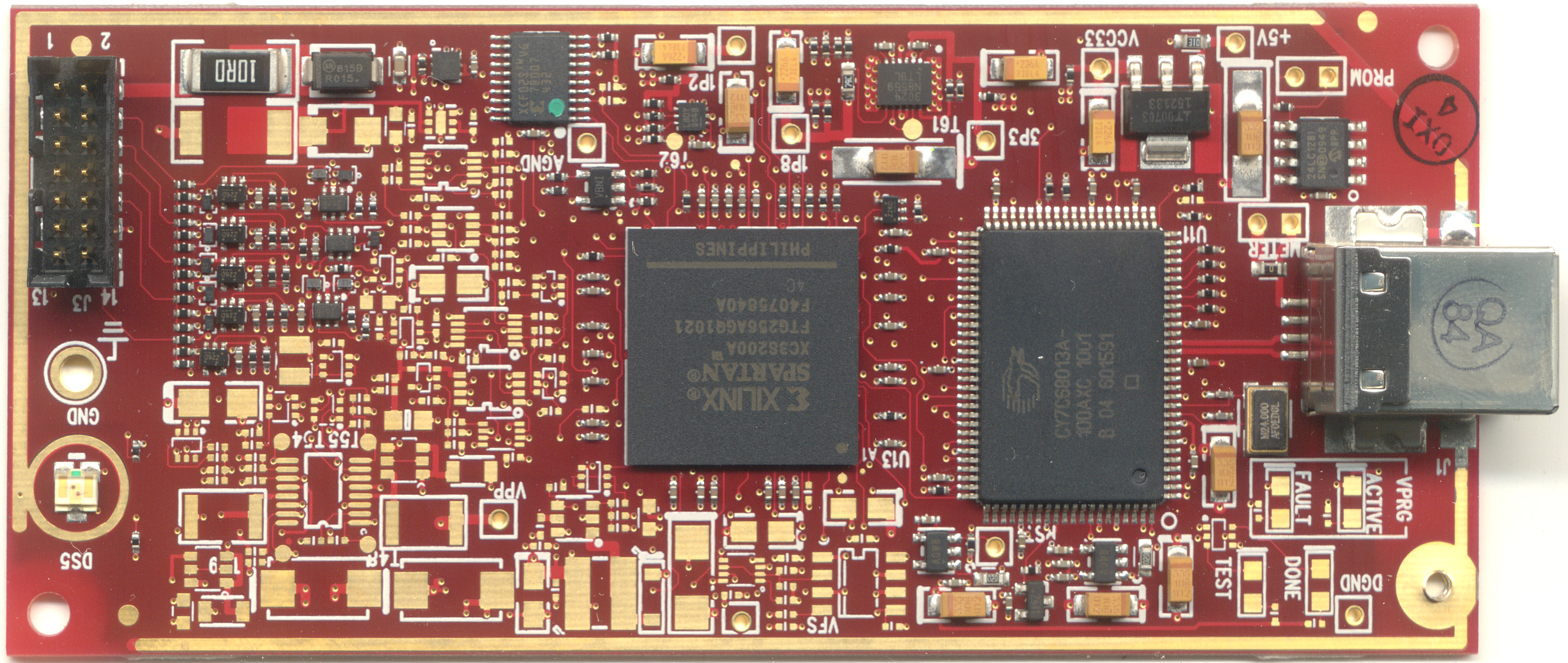
My first step in deciding how to proceed was to see what made their adapter tick. I would have opened up the adapter to see what was inside, but Bunnie saved me the trouble by posting pictures a while ago as the Name That Ware for March 2011.

Xilinx Platform Cable USB II (image courtesy of Bunnie)
The vast majority of the footprints on the board aren't even populated... one can only guess what additional functionality may have been planned at one point. There's an XC3S200A FPGA, a Cypress USB MCU, USB descriptor EEPROM, flash for the FPGA, and then a bunch of passives for power regulation and level shifting. Overall, the design is quite simple and certainly not worth $250.

After browsing for something cheaper and based on a well-known chipset, I found the Digilent HS1, a $54.99 FT2232-based adapter which is supported by Digilent's documented JTAG API and integrated nicely with the Xilinx IDE. In addition, since it's a standard FTDI chipset it would be possible to interact with it at a lower level using libftd2xx. (I also built a custom FT232H-based programmer that I have half a dozen of around my lab, but I wanted a known-good design to verify my software on first.)

The HS1 worked quite well using the Xilinx tools, but I still needed JTAG code to talk to it and interact with the FPGAs for scripted tests. I looked at a couple of popular options and rejected each of them:
  • OpenOCD (GNU GPL, incompatible with the BSD license used by my work)
  • xc3sprog (GPL, standalone tool with no API, includes programming algorithms that can run directly off a .bit file)
  • urjtag (GPL, has a socket-based JTAG server under development but not released yet)
It looked like I was going to have to write my own software, so I sat down and did just that. The result was a C++ library I call libjtaghal (JTAG hardware abstraction layer). It will be released publicly under the 3-clause BSD license once I've cleaned it up a bit; in the meantime if anyone wants a raw code drop with no documentation and a not-quite-finished build system leave a comment and I'll post something.

The basic structure of libjtaghal is built around two core object types: interfaces and devices. A JtagInterface represents a connection to a single JTAG adapter. As of now I support:
  • FT*232H MPSSE (assumes ADBUS7 is the output enable, an option to configure this is planned for the future)
  • Digilent API (for HS1 and integrated programmers on the Atlys etc)
  • Generic socket-based protocol for talking to remote libjtaghal servers
My custom 8-port JTAG system (more to follow in a future post) will use my socket-based protocol and show up as 8 separate interfaces which can each be controlled independently (potentially from 8 separate client PCs).

 A JtagDevice represents a single chip in a scan chain. Support for multi-device scan chains needs a bit more work; this is one of the reasons I haven't released it yet.

A given JtagDevice may implement one or more additional interfaces. Some of these are:
  • CPLD (generic complex programmable logic device)
  • FPGA (generic FPGA device)
  • ProgrammableDevice (any device which accepts firmware of some sort, including CPLDs, FPGAs, MCUs, and JTAG-capable ROMs)
  • RPCNetworkInterface (a device which supports sending RPC messages over JTAG)
  • DMANetworkInterface (a device which supports sending DMA messages over JTAG)
  • RPCAndDMANetworkInterface (implements RPCNetworkInterface, DMANetworkInterface, and some logic to connect the two protocols)
This design allows several very handy design abstractions. For example, the below code is the sum total of the "program" mode for my "jtagclient" command-line application. It takes a JtagInterface object "iface" and programs the device at chain index "devnum" with the firmware image "bitfile". Note the complete lack of any device- or interface-specific code. The same function can configure a CoolRunner-II via one of my custom FTDI programmers or a Spartan-6 using the integrated Digilent programmer on a dev board without changing anything.

JtagDevice* device = iface.GetDevice(devnum);
if(device == NULL)
{
 throw JtagExceptionWrapper(
  "Device is null, cannot continue",
  "",
  JtagException::EXCEPTION_TYPE_BOARD_FAULT);
}

//Make sure it's a programmable device
ProgrammableDevice* pdev = dynamic_cast(device);
if(pdev == NULL)
{
 throw JtagExceptionWrapper(
  "Device is not a programmable device, cannot continue",
  "",
  JtagException::EXCEPTION_TYPE_BOARD_FAULT);
}

//Load the firmware image and program the device
printf("Loading firmware image...\n");
FirmwareImage* img = pdev->LoadFirmwareImage(bitfile);
printf("Programming device...\n");
pdev->Program(img);
printf("Configuration successful\n");
delete img;

This is part of the test case for my gigabit Ethernet MAC, allocating a page of memory on the device under test by talking to the RAM controller at NoC address "raddr" via the RPCNetworkInterface "iface". (Details on how this is implemented will be coming in a few posts.)

printf("Allocating memory...\n");
iface.RPCFunctionCall(raddr, RAM_ALLOCATE, 0, 0, 0, rxm);
uint32_t txptr = rxm.data[1];
printf("    Transmit buffer is at 0x%08x\n", txptr);

There's a lot more to the system than this but I'll save the rest for my next post :)